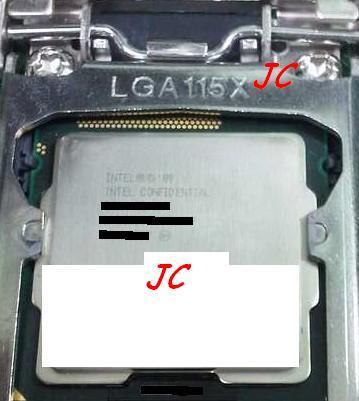
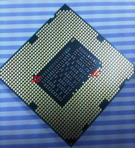
We’ve been hearing rumors of Intel’s next generation processors platform LGA 115X. Intel has revealed shipping thousands of Sandy Bridge processors to partners for evaluations and it therefore comes as no surprise one of them got lost. JCornell has once again managed to get a hold of Intel’s fresh products and published screenshots and pictures with information on the new processor.
Sandy Bridge will be a new architecture and as a “tock” in Intel’s processor roadmap it is based on the “old” 32 nanometer technology.
The big difference between today’s mid-range processors with 32nm technology is that Sandy Bridge has the GPU inside the die, which also means the whole circuit is made with 32nm technology, not like Clarkdale where the graphics portion is 45nm.
The new LGA 115X socket is not compatible with the current LGA 1156 socket and the processor JCornell has in his possession shows 100MHz base clock instead of the 133MHz of both LGA 1156 and LGA 1366.
We have confirmation that the processor has dual cores and HyperThreading, and that Intel has revised the cache of the microarchitecture. It has reduced the amount of L3 cache to 3MB that now has a narrower interface (12-way associative), compared to 4M and 16-way of Clarkdale. The L1 instruction cache is wider instead, 8-way instead of 4-way, Clarkdale.
The processor seen on the pictures operate at 2.4GHz with 0.986V operating voltage. Whether this is a setting that will make it to market or not is hard to say considering we’re so far off the launch, we’re betting the frequency will be higher.

Whether Sandy Bridge really offers 20% higher performance than the mobile Arrandale platform remains to be seen, but with its truly integrated graphics processor Intel has great chances of lowering power consumption further, which is highly welcomed with the mobile segment.


