AMD’s sucessor to Llano is starting to take shape and today a picture of the circuit has given us many of the details we have been speculating in. Trinity will like Llano be based on something slightly older, and something new from AMD, including the processor portion that is based on the Bulldozer architecture.
Llano turned out to be AMD’s most popular product in a long time and since the launch suffered from poor availability in stores and to partners. What disappointed many enthusiasts was the fact that Llano was based on old technology in many ways, with a slightly updated processor cores from Phenom II and graphics architecture from Evergreen.
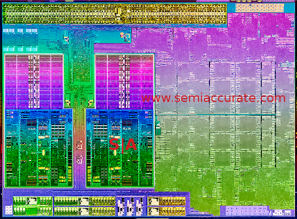
From that perspective Trinity looks a lot more interesting, and thanks to the first picture more details have come to the surface.
Trinity sports two Piledriver modules housing two cores eacg, for a total of four processor cores. Each module will get 2 MB L2 cache, same as Bulldozer as Piledriver. Hopefully AMD has done better with Piledriver than the energy consuming Bulldozer. The memory controller is still a dual-channel DDR3 with a 128-bit memory bus, but Trinity should still be able to supply the graphics circuit with more bandwidth thanks to the support for higher clock frequencies. It is sitll unclear if Trinity supports PCI Express 3.0, or if it is stuck at PCI Express 2.0.
The graphics in Trinity will be based on AMD’s VLIW4 architecture that is used in the HD 6900 series and the Cayman circuit. According to the picture above it looks like it will get six VLIW4 cluster for a total of 384 Radeon cores, which is less than Llano’s 400 cores that uses five VLIW5 clusters. The VLIW4 architecture is more efficiency and together with support for higher memory frequencies and overall higher frequencies we should expect better graphics performance from Trinity than Llano. Trinity also supports the dedicated H.264 decoder VCE, just like the graphics cards of the HD 7000 series and the new GCN architecture.
| Circuit | Trinity | Llano |
| Node | 32nm SOI/HKMG | 32nm SOI/HKMG |
| Architecture | Piledriver | Stars |
| Modules | 2 | – |
| Cores | 4 | 4 |
| L2 cache |
2 x 2 MB | 4 x 1 MB |
| Graphics architecture |
VLIW4 (6 kluster) | VLIW5 (5 kluster) |
| Radeon cores |
384 | 400 |
| Decoding functions |
UVD3 / VCE | UVD3 |
| Size | 240 mm² | 228 mm² |
All this aside, AMD has improved the Power-gating to be able to turn off more functions when they are not needed and thus reduce energy consumption. Trinity will not be a large chip either, but about 240 mm², which is just slightly bigger than Llano at 228 mm². It has been revealed that Trinity will come in three configurations, and we assume that the one above will be the top model used in the A10 and A8 series. Even if Trinity looks good on paper it will go up against Intel Ivy Bridge, which will bring new graphics and Intel’s new 22nm technology.
Source: Semiaccurate


