


The world is preparing itself for the new 28nm processors from TSMC, GlobalFoundries and Samsung, and while it does on the companies continue to develop the future replacements. TSMC and ARM have now take the first step toward 20nm by etching out the first real circuit.
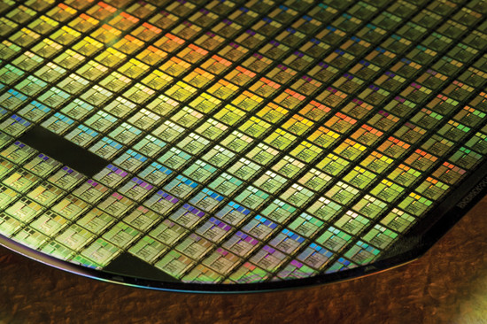
TSMC and ARM hav had its first tape-out of a real circuit. The first that happens with a new node is that you develop transistors and a wafer, and simpler SRAM logic. They are not for retail, but only for internal tests to find bugs and make sure the process can produce viable circuits.
ARM was one of the first partners to test 20nm at TSMC, and it has squeezed out its first Cortex-A15 MPCore at 20nm. ARM mentions no details if it is a single core or if it has logics built around it. ARM is one of the most important partners a foundry can have since it’s technologies are used in all kinds of circuits, so it is important that the processor cores and logics is well adjusted to the foundry nodes.
With the first real step on 20nm, ARM will now start optimizing its physical IP together with TSMC to reduce the die size, energy consumption and improve performance. It doens’t say when th 20nm process will be ready for retail clients and products.
We know since earlier that GlobalFoundries will start its production at 20nm during 2012, while the launch will take until later. The 20nm-LPM (Low Power Manufacturing) node for smaller and energy efficient circuits like smartphone SoCs will launch in 2013, while 20nm-SHP (Super High Performance) will launch in 2014. We can only assume that TSMC has a similar schedule now that GlobalFoundries is starting to get a better grip on the market and more attention among the industry people.
Source: EETimes


