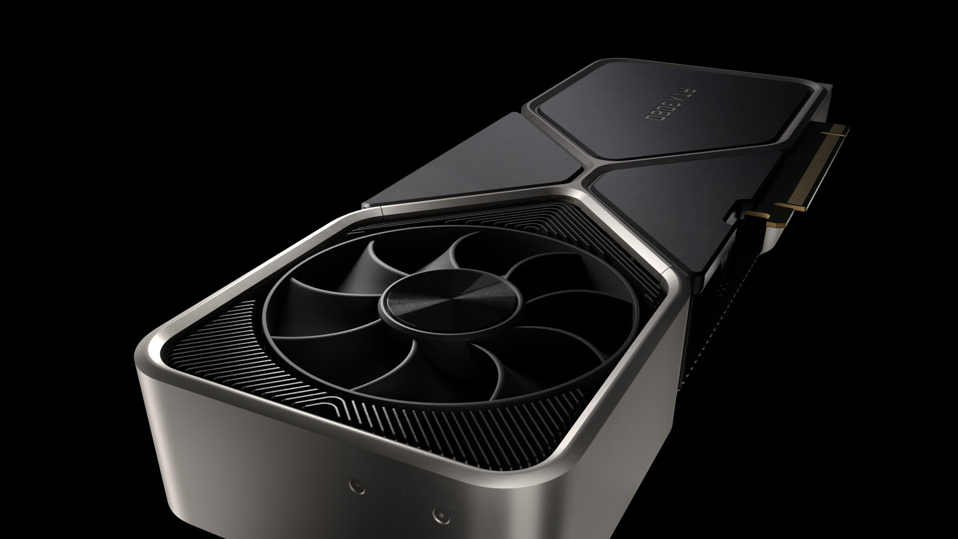
NVIDIA hasn’t made any revolutionary changes to its recently launched GF110 GPU. The optimizations it did do brought back the Fermi architecture and made it more competitive. This is something it will continue to build on with a new flag product, GeForce GTX 570 that will launch in December.
GeForce GTX 570 looks to be the last nail in the coffin for NVIDIA’s former flagship GeForce GTX 480. NVIDIA has deactivated one of the 16 SM units of the GF110 circuits which gives GTX 570 the same number of CUDA cores as the previous flagship, 480. At the same time it will borrow the uneven 320-bit memory bus from GeForce GTX 470 and connect it to 1280 MB GDDR5 memory.
The exact clock frequencies doesn’t seem to be certain yet, but according to the latest rumors we’re dealing with 690 MHz GPU clock, shaders at 1380 MHz and GDDR5 memory at effective 3800 MHz. Even if these numbers should be taken with a pinch of salt they would result in the following table.
| GeForce GTX 580 | GeForce GTX 570 | GeForce GTX 480 | GeForce GTX 470 | |
| GPU | GF110 | GF110 | GF100 | GF100 |
| Node | 40nm | 40nm | 40nm | 40nm |
| CUDA cores |
512 | 480 |
480 | 448 |
| GPU clock freq. |
772 MHz | 690 MHz | 700 MHz | 607 MHz |
| CUDA clock freq. |
1 544 MHz | 1 380 MHz | 1 400 MHz | 1 215 MHz |
| Memory clock freq. |
4 008 MHz | 3 800 MHz | 3 696 MHz | 1 674 MHz |
| Memory interface |
384-bit | 320-bit | 384-bit | 320-bit |
| Memory buffer |
1 536 MB | 1 280 MB | 1 536 MB | 1 280 MB |
| Memory bandwidth |
192,4 GB/s | 152,0 GB/s | 177,4 GB/s | 133,9 GB/s |
| Texture fillrate | 49,4 GTexel/s | 41,4 GTexel/s | 42,0 GTexel/s | 34,0 GTexel/s |
Power consumption is said to be on the same level as GeForce GTX 470, but around 20% better performance. This would make it the perfect partner to GTX 580 when AMD launches its new top models in December, Radeon HD 6970 and HD 6950.
Source: Expreview


