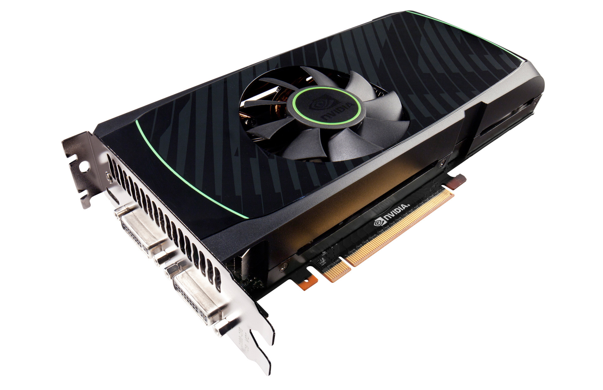
GeForce GTX 680 looks to be the name of NVIDIA’s first graphics card in the Kepler family and the card is expected to launch March 23rd, and the specifications have now surfaced. According to the latest rumors we will have plenty of CUDA cores and really fast GDDR5 memory.
NVIDIA’s first graphics circuit with 28 nanometer technology will be called GK104 and takes aim for the performance segment. It is not the most powerful circuit NVIDIA has to offer from the Kepler family, but performance will be sufficient to to put it on par with GeForce GTX 580. According to VR-Zone the final specifications for GeForce GTX 680 – the name(?) of the GK104 top model – has been revealed.
According to these rumors NVIDIA has focused more on more cores and filled the GK104 circuit with 1536 CUDA cores, which is three times more than GF110 at 512 CUDA cores. NVIDIA will according to VR-Zone continue to use asynchronous frequencies where the GPU logic operates at 705 MHz, while the 1500 CUDA cores operate twice as fast at 1411 MHz.
The memory bus is limited compared to the GeForce GTX 500 series, but the 256-bit wide memory bus works with 2GB GDDR5 memory at 6000 MHz, a new record for a reference card. The memory bandwidth lands at 192.4 GB/s, which is identical to GeForce GTX 580. There is no information on the number of texture units or ROPs, but according to estimates the GK104 GPU will measure ~320mm².
| Model | GTX 680 “Kepler” | GTX 580 “Fermi” | HD 7870 “Southern Islands” |
| GPU | GK104 | GF110 | Pitcairn XT |
| Technology | 28nm | 40nm | 28nm |
| Die size |
320mm² | 520mm² | 212mm² |
| CUDA/Radeon cores |
1536 st | 512 st | 1408 st |
| GPU frequency |
705 MHz | 772 MHz | 1000 MHz |
| Shader frequency |
1411 MHz | 1544 MHz | – |
| Memory |
2GB GDDR5 | 3 GB GDDR5 | 2 GB GDDR5 |
| Memory bus |
256-bit | 384-bit | 256-bit |
| Memory freqency |
6.0 GHz | 4.0 GHz | 5.0 GHz |
| Memory bandwidth |
192 GB/s | 192 GB/s | 153.6 GB/s |
| ROPs | ? | 32 | 24 |
| Texture units |
? | 128 | 88 |
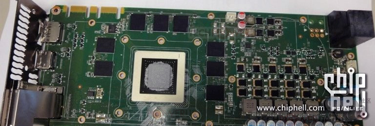
GeForce GTX 680 will be 25.5 cm long and use dual PCIe power connectors, either 2×6 pins or 1×6 pin + 1×8 pin. VR-Zone mentions that the stacked connectors seen on leaked pictures will probably not make it to retail. Other specifications include dual DVI ouputs and HDMI and DisplayPort ports.
The launch of NVIDIA’s new performance card GeForce GTX 680 will according to VR-Zone happen on March 23rd, but that already on March 12th the company will reveal more about the new graphics circuit.
Source: VR-Zone


Sorry, but your chart has some MAJOR errors:
GTX580 has 48 ROPs not 32

GTX580 has 64 TMUs not 128
HD7870 has 32 ROPs not 24
HD7870 has 80 TMUs not 88
HD7870 has 1280 SPs not 1408
http://www.anandtech.com/show/5625/amd-radeon-hd-7870-ghz-edition-radeon-hd-7850-review-rounding-out-southern-islands/1
Also, the rumored # of ROPs is 32 for GTX680 and 128 TMUs.
Also, GK104 will be GTX 670 Ti, not GTX 680, which will be GK110.
asdsafs, Rumors have it GK104 is the real GTX680. Nvidia is going to release GK110 as the next generation GTX780 since GK104 is sufficient enough to beat a stock HD7970. This means NV will be milking consumers just like AMD is doing now, selling us 320-340mm^2 die space GPU for $500+. You get the feeling AMD purposely released an underclocked 925mhz HD7970 and NV is purposely holding back GK110. AMD probably realized the insanely low priced in HD4800/5800/6900 series destroyed their margins/profits. I mean HD4870 for only $299, HD5870 for $379 and HD6950 unlocked into a 6970 for ~$250 market… Läs hela »
Ya, the GK110 is supposed to be the GTX680, not the GK104. The GTX680 is supposed to be 2000~ cores.