


GlobalFoundries continues to show that it wants to become a force to reckon with in the foundry business and has presented two technologies at the 20nm node that will debut in 2013 and 2014. It ensures that also SOI will have a future support, but there are no new customers for SOI besides AMD.
At GTC (GlobalTechnology Conference) GlobalFoundries presented its planned technologies at 20nm, that will follow and replace 28nm and 32nm. The 20nm node will come in two versions adjusted depending on the customer and circuit.
The first news is that at 20nm it will go from Gate-First to Gate-Last. Gate-First gave GlobalFoundries 10-20% less circuit space, but according to other people in the industry it is hard to master. GlobalFoundries says that it has chosen Gate-Last after analyzing the market and believe that circuit space will not be the top priority of its clients.
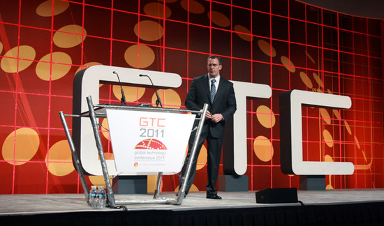 Greg Bartlett, GlobalFoundries at GTC 2011
The 20nm node comes in two shapes, 20nm-LPM (Low-Power Manufacturing) for smaller more efficient circuits like smartphone SoCs, while 20nm-SHP (Super High Performance) will target high-end circuits like graphics processors. Both technologies sport HKMG and is estimated to end up below 0.9V, compared to right above 1.0V for 28nm and 32nm.
20nm-LPM will bring great improvements over 28nm-ULP, and will offer up to 35% faster circuits at the same energy consumption level, or up to 40% lower energy consumption with the same performance. 20nm-SHP will bring 25% faster circuits, or 30% lower energy consumption. Both 20nm versions will bring double the transistor density of 28nm.
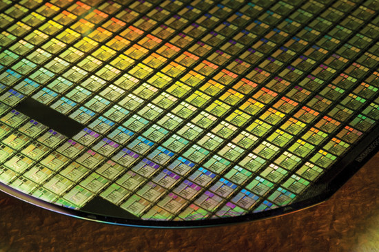
A wafer is a round disc that takes 8-12 weeks to make, the circuits are then cut with lasers and packaged for used in a computer of some sort.
The company has produced test wafers, and 20nm is available for client evaluation. It will start 20nm production by the end of 2012, while it will launch in two stages in 2013 and 2014. In 2014-2015 the company will debute its first prototype node based on EUV (Extreme Ultra Violet) and prepare a transition from the traditional CMOS transistor. What we will get after that is most likely so called 3D transistors that Intel will introduce at 22nm next year.
INterim VP Ajit Manocha expressed himself incorrectly and gave birth to a rumor that GlobalFoundries will not support SOI (Silicon-on-Insulator) anymore, which he has now corrected. SOI that AMD uese is still on the map and it is fully committed to SOI. The processes based on SOI that have been decided at GlobalFoundries is 22nm and 14nm, and it is likely that it will continue even lower if AMD manages to bring enough orders in.
Tri-Gate transistors that Intel will implement is just one of many means to remedy current leakage.
We can’t help keeping an eye out for what 20nm will produce. It is a substantial increase although smaller than before, a testament to that we are getting closer to the physical limitations of the silicon-based transistor and that current leakage is getting tough to control. Technologies like HKMG, FinFet (3D), SOI, EUV are not performance enhancing means, but just a way to plaster the leakage. It is starting to become clear that silicon doesn’t have many uears to go, especially since it is looking impossible to go below 10nm.
Source: BrightSideOfNews


