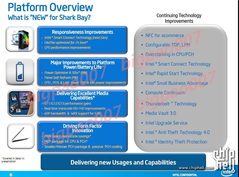
Haswell is Intel’s coming arhictecture to replace Ivy Bridge in 2013, and just like rumors have suggested it will be something of a SoC design (System-on-a-Chip) for ultramobile units. The focus with Haswell is on mobility and energy efficiency.
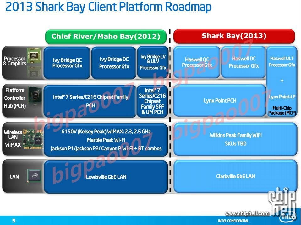
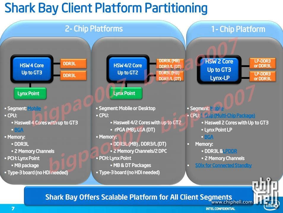
We reported a while back that Haswell will use a SoC design, with larger focus on graphics then before. The new platform for Haswell will be called Shark Bay, but unlike both Sandy Bridge and Ivy Bridge it will come in two shapes depending on the market. One will be traditional, a processor with bundled southbridge on the side, and one with the southbridge included in the silicon package.
 |
 |
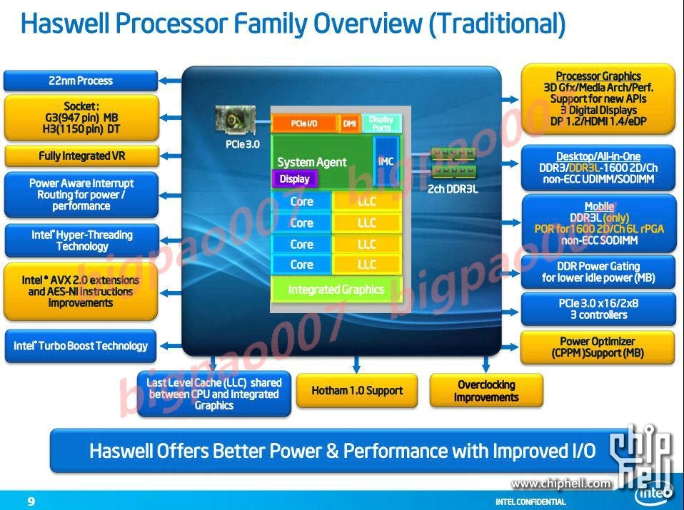
If we start with the first deal, Shark Bay with processor and southbridge will sport two or four cores. The desktop models will bring 35W, 45W, 65W or 95W TDP and GT2 graphics, while the mobile versions will bring 37W, 47W and 57W TDP and more powerful GT3 graphics. The exact differences in the graphics circuits is unclear, but the mobile versions will be the ones with more potential.
Also a weaker GT1 graphics circuits will be available, most likely in desktop entry models. Intel’s new graphics architecture will support technologies like Intel WiDi and stereoscopic 3D. Performance is clouded, but should be better than Ivy Bridge that is rumored to be on par with AMD A6. Southbridge will support more technologies than before, and that includes Intel Thunderbolt.
 |
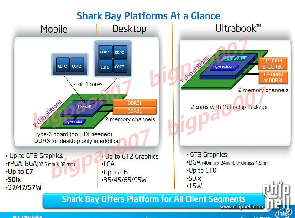 |
In the second shape we mentioned, Intel’s SoC-version of Haswell targets Ultrabooks. Ultrabook Haswell will sport GT3 graphics, two cores and TDP up to 15W, which paired with better energy efficiency could become really interestin. Intel is doing its own version of SoC it calls a Multi-chip Package, a technology already used by the Atom circuits.
The technology works so that you make the circuits separate from each other, but then join them into a single package. The advantages of this is you can faster and more easily change components in the SoC. If intel decides to update the southbridge in the future it can just swap the part instead of redesigning the entire package. The reason Intel has used a SoC design is to reduce the overall size of the platform, to enable even thinner and smaller designs.
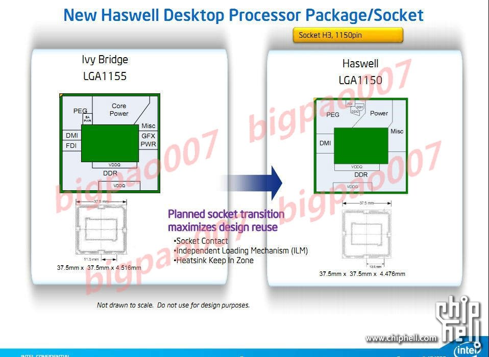 With a new Tick from Intel with the new Haswell architecture comes a new socket. It will be socket LGA1150 that is similar to LGA1155 in many ways. For example, coolers for LGA1155 will be compatible with LGA1150.
Haswell will be Intel’s first whole new architecture in a long time, and it is starting become all the more clear that Intel has bet on energy efficiency and mobility. Much of the work has gone into reducing energy consumption of an idle processor or under low loads. Also to speed up in the blink of an eye to update social media, e-mail and documents is in focus.
Haswell will be built on the 22nm process and considering Intel’s Tick-Tock strategy we can expect Haswell around Q2 2013. The sequel to Haswell will be called Broadwell and arrive at 14nm, with launch in the same period in 2014 if the transition to the new node works as intended. What we do know is that Intel is focusing all the more on mobility in the future.
Source: Chiphell


