Great ideas are high value in the NAND Flash business where the memory makers are running into one obstacle after another. The perhaps biggest obstacle is the limited lifespan of NAND memory circuits, which is becoming a bigger problem with each new node. It seems we need new packaging for the next level of performance.
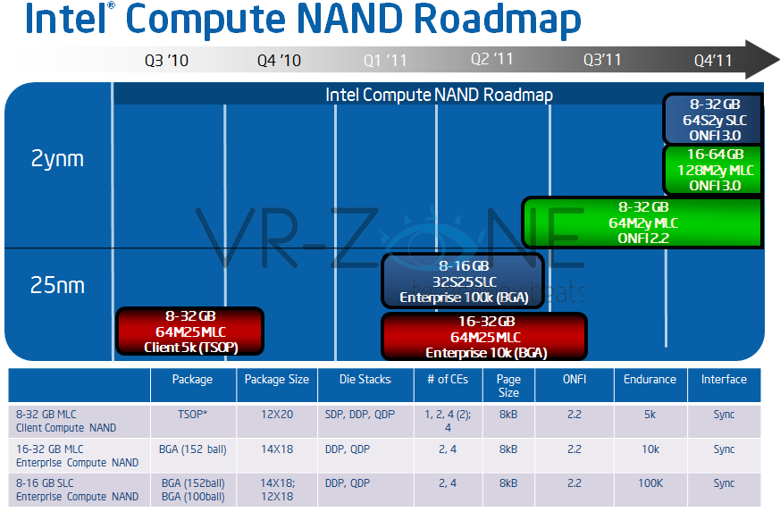
Intel has started the transition from the classic and more cost efficient TSOP (Thin Small-Outline Package) to the more expensive, but also more advanced BGA package (Ball Grid Array). The business products are first in line, where it has already started making 25nm NAND in BGA packages.
The reason Intel is said to switch to BGA NAND circuits is the coming NAND standard ONFI 3.0. With up to 400MB/s per chip bandwidth the less advanced TSOP technology becomes a bottleneck and especially in the business segment where the cost margins are larger Intel is preparing BGA circuits with better outlooks.
According to a roadmap published at VR-Zone we see that Intel has since Q1 2011 started to roll out BGA 25nm NAND circuits for the business segment, for the ONFI 2.2 standard. In Q4 Intel is expected to introduce 20nm NAND circuits that adhere to the ONFI 3.0 standard and most likely only in BGA suits.

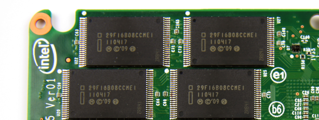
NAND circuits made in TSOP and BGA packages
Regular retail products will be upgrader later on and this is most likely because of the higher production costs of BGA. How Intel and other NAND companies will solve this is unclear, but TSOP for NAND flash is most likely becoming a thing of the past, for performance products at least.


