Intel stretches the limits with the 22 nanometer technology
Intel’s position on the market in manufacturing processes is nothing short of impressive. While we can see that the other actors within the semiconductor industry is right now migrating to the 32 and 28 nanometer technologies, meanwhile for Intel that is today history. They have for months begun massproducing processors on the new 22 nanometer technology, with a new kind of groundbreaking transistors that others only has experimented with so far and not put into commercial use.
The so-called 3D-transistor from Intel has been on the wall ever since they started talking about it officially in May last year, but what exactly is this 3D-transistor or as the proper name for the technology is called; Tri-Gate? The transistors is not much more three dimensional than before, but at the same time it’s not completely wrong to claim that Intel has added a third dimension to the transistor.
The trouble with smaller transistors
A transistor basically works as a switch with two positions – 1(on) and 0(off). When the transistor is set to 1, as much current as possible should be able to flow through it, and when it’s set to 0 as little current as possible should flow through it – it would be best if you could stop the flow completely. If that wasn’t enough a transistor has to be able to be switched between off and on as fast as possible. The number of times a transistor is switched between off and on per second is what we call clock frequency. The processor we are reviewing today is Intel Core i7-3770K which has a clock frequency of 3,5 GHz (GigaHertz), that means the transistors in the processor cores switches between off and on 3,5 billion (3 500 000 000) times per second.
We can shrink transistors and place more of them at the same space as before – the current, or more correctly the electrons isn’t that easy, or downright impossible to shrink. Our beloved electrons has always had the same size and will always have the same size. The chase for faster processors make the electroncs bigger and bigger in proportion to the transistors, and sometimes “disappear” from their decided path. This is the devious current leakage that we nag about every time a new manufacturing process is being brought up, and the problem just continues to grow. This is one of many reasons that we don’t get the same results from new manufacturing processes today like we did several years ago – we’re getting closer and closer to the point where the laws of physics just says no.
High-K Metal Gate – one of many technologies
We have for a long period of time tried to apply bandaid to and minimize the current leakage, with good results. Bulk and Silicon-on-Insulator (SOI) were introduced many years before this, while HKMG(High-K, Metal Gate) is one of the more recent.
Silicon dioxide (SiO2) had earlier been used between the transistor gate and the flow of current to switch the transistor on and off. As we gradually shrunk our transistors further the silicon dioxide layer became thinner and thinner, which in turn resulted in a quantum phenomenon which is called Quantum Tunneling. The number of transistors that the silicon dioxide layer was built of became so thin that the electrons managed to squeeze themselves through places where it shouldn’t be possible.
 Intel Penryn – the worlds first commercial circuit with HKMG
Intel was first in the world to introduce HKMG, and they chose haufnium dioxide (HfO2) to replace the silicon dioxide. Aside from higher capacitance, the current leakage was significantly lowered. Without technologies like these, the silicon dioxide that we build our processors and circuits on would literally have burned up as soon as we would have powered on our computers or any type of electronics that we use for that matter. In other words, it’s no increase in performance that we’re talking about, but an absolute must in the chase for higher performance and lower power consumption.
Tri-Gate – the next evolutionary step
Tri-Gate is yet another technology to curb the current leakage and has a great resemblance to FinFET, even if Intel officially won’t admit it. In our interview with Intel’s European Managing Director, Patrick Bliemer, we discussed their 22 nanometer technology but also their upcoming 14 nanometer technology which as expected will go to mass production during the first 6 months of 2014. Unfortunately this was a part that didn’t make it to our article about the interview so we will take it here instead.
We asked the question if Tri-Gate really was necessary on 22 nanometer – could it have been done without the technology? Not all foundries will begin using 3D-transistors before 14 nanometer, so the same should apply to Intel. The answear we got was that it would absolutely have been possible, but Intel wouldn’t have been pleased with the result. Tri-Gate also raises the costs for manufacturing, but according to Bliemer the advantages outweigh the disadvantages. The total raise in manufacturing costs are between two and three percent. Intel also considered SOI but that would have increased the cost by ten percent.
So what makes the transistor so special?
What is Intel’s Tri-Gate transistor really? The transistors used everywhere today is what we call “Planar transistors”, thus of course meaning planar transistors. The planar transistors has a planar surface where the current can flow (Inversion Layer), and over that is a gate which has the mission to switch the transistor off and on. What the Tri-Gate transistor does is that it can switch off and on the current in a transistor from three different dimensions, as the inversion layer is now a fin that has been raised.
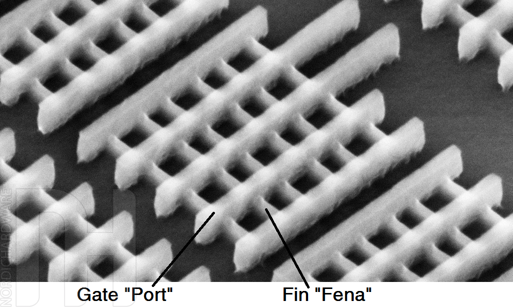
 Intel’s Tri-Gate transistors on 22 nanometer under the microscope
In the above comparison Intel’s Tri-Gate transistor only has one fin, but depending on the area of use several fins can be used. The result of several fins is that more current can flow through it when it is needed, which in turn leads to potentially higher performance. The faster parts of the processor can have transistors equipped with several fins while parts that will run on a relatively low clock frequency can do what it’s supposed to with just one.
 A planar 32 nanometer transistor, side-by-side Intel’s 22 nanometer transistor with the fin to the right
The gate that switches off and on is now surrounding the fin from three different directions, which results in a less current leakage when the transistor is switched off. The advantage of several fins can raise the clock frequencies to new heights. They have also succeded to improve the transistor in the three most important areas:
- Higher current flow
- Lower current leakage
- Higher clock frequencies (faster on and off switching)
The technology itself is promising if we’re to trust Intel’s data. The new manufacturing process that the Tri-Gate transistor is built on should with a 0,7V lower voltage, increase the performance with 37 percent with the same power consumption as before. If you raise the voltage by 1,0V, the increase in performance would be 18 percent. This means that we will get to see the biggest difference on the companies mobile products with the help of the new transistor, not to mention the new 22 nanometer manufacturing process.


Great review guys, i would really love to see you do much more of them =]
A really great review, good job. Waiting to get my hands on it… but don’t know when it will arrive in Brazil
Glad you liked it
We hope the new translators will have time for more of these.
You used DDR3-1333 for AMD APU when it’s known that those processors need faster RAM to reach top performance, unlike Intel’s which don’t scale up accordingly. As it is, this is a very Intel-biased review.
[quote name=”Taki R”]You used DDR3-1333 for AMD APU when it’s known that those processors need faster RAM to reach top performance, unlike Intel’s which don’t scale up accordingly. As it is, this is a very Intel-biased review.[/quote]If you’re talking about CPU performance, the difference is very much negligible. I can agree however if we’re talking GPU-performance, where may I add, even Ivy Bridge HD 4000 benefits from higher RAM-clocks as well so it’s pretty much apples-to-apples in that regard. We will be revising our testing methodology during the summer, so we’ll be taking all of these things into close consideration… Läs hela »
It seem Intel will beat AMD more with this line of new generation processor. It is faster and consume less power than sandy bridge and trinity. Core per core / clock per clock basis.
I really like to know though the performance and efficiency compare to AMD trinity.
É realmente incrível todo esse progresso/evolução da INTEL.
BRASIL – CRATO – CEARÁ
É realmente incrível todo esse progresso/evolução da INTEL.
BRASIL – CRATO – CEARÁ
What happens if I put a 125w TDP CPU on a 95w motherboard? If I have a quad-core CPU and disable 2 cores will my CPU fit in the 95w TDP?