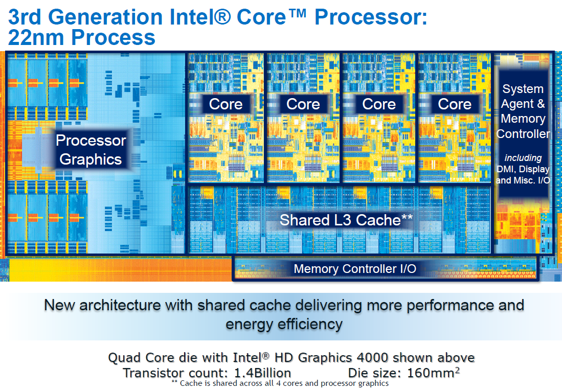
1,4 billion transistors at only 160mm²
Ivy Bridge will be the first 22 nanometer based circuit in the world and today it looks like Intel will have a continued advantage for the next few years. Intel has with their new manufacturing process increased the transistor count by approximately 40 percent in comparison to Sandy Bridge and at the same time managed to shrink the circuits surface area from 216 mm² to only 160 mm².
| Feature | Cores | L2 cache | L3 cache | Technology | Transistors | Circuit area |
| Ivy Bridge | 4 | 4 x 256 KB | 8 MB | 22nm Bulk/HKMG/Tri-gate | 1 400 mil. | 160 mm² |
| Sandy Bridge | 4 | 4 x 256 KB | 8 MB | 32nm Bulk/HKMG |
995 mil. | 216 mm² |
| Sandy Bridge-EP | 8 | 8 x 256 KB | 20 MB | 32nm Bulk/HKMG |
2 270 mil. | 435 mm² |
| Sandy Bridge-E | 4 | 4 x 256 | 10 MB | 32nm Bulk/HKMG |
1 270 mil. | 294 mm² |
| Zambezi | 8 | 4 x 2 MB | 8 MB | 32nm SOI/HKMG |
~2 000 mil. | 315 mm² |
| Thuban | 6 | 6 x 512 KB | 6 MB | 45nm SOI/HKMG |
904 mil. | 346 mm² |
| Llano Wintercreek | 2 | 2 x 1 MB | – | 32nm SOI/HKMG |
758 mil. | ? |
| Llano Beavercreek | 4 | 4 x 1 MB | – | 32nm SOI/HKMG |
1 450 mil. | 228 mm² |
| Westmere | 6 | 6 x 256 KB | 12 MB | 32nm Bulk/HKMG |
1 170 mil. | 240 mm² |
| Sandy Bridge | 2 | 2 x 256 KB | 4 MB | 32nm Bulk/HKMG |
624 mil. | 149 mm² |
| Sandy Bridge | 2 | 2 x 256 KB | 3 MB | 32nm Bulk/HKMG |
504 mil. | 131 mm² |
| Regor | 2 | 2 x 1 MB | – | 45nm SOI |
234 mil. | 117 mm² |
| Propus | 4 | 4 x 512 KB | – | 45nm SOI |
300 mil. | 169 mm² |
| Deneb | 4 | 4 x 512 KB | 6 MB | 45nm SOI |
758 mil. | 258 mm² |
| Penryn | 2 | 6 MB | – | 45nm Bulk/HKMG |
410 mil. | 107 mm² |
| Bloomfield | 4 | 4 x 256 KB | 8 MB | 45nm Bulk/HKMG |
731 mil. | 263 mm² |
| Lynnfield | 4 | 4 x 256 KB | 8 MB | 45nm Bulk/HKMG |
774 mil. | 296 mm² |
| Clarkdale | 2 | 2 x 256 KB | 4 MB | 32nm Bulk/HKMG |
383 mil. | 81 mm² |
While Ivy bridge is just a Tick in Intel’s Tick-Tock schedule they have still made a major increase in transistors. In every Tick Intel makes small changes and adjustments to get higher performance and power effiency, also fixing bugs in the architecture. Although that’s not enough to cover and justify a 40 percent increase.
In the new Gen 7 graphics architecture which is a development of their Gen 6 architecture and can be found in Sandry Bridge, Ivy Bridge comes with an improved integrated graphics circuit. The idea is to offer as much as possible, and in the future everything that’s needed in a computer on one single piece of silicon.
What we can expect in the future is a similar trend that will continue. Instead of making everything as tiny as possible the new manufacturing processes will be used to continue the integration of several components on one die. The integer unit, the memory controller, the northbridge and the graphics is just a few of the parts that has been built into the processor. At this point it’s just a matter of time before the southbridge will be built in – and in time even the RAM-memory.








Great review guys, i would really love to see you do much more of them =]
A really great review, good job. Waiting to get my hands on it… but don’t know when it will arrive in Brazil
Glad you liked it
We hope the new translators will have time for more of these.
You used DDR3-1333 for AMD APU when it’s known that those processors need faster RAM to reach top performance, unlike Intel’s which don’t scale up accordingly. As it is, this is a very Intel-biased review.
[quote name=”Taki R”]You used DDR3-1333 for AMD APU when it’s known that those processors need faster RAM to reach top performance, unlike Intel’s which don’t scale up accordingly. As it is, this is a very Intel-biased review.[/quote]If you’re talking about CPU performance, the difference is very much negligible. I can agree however if we’re talking GPU-performance, where may I add, even Ivy Bridge HD 4000 benefits from higher RAM-clocks as well so it’s pretty much apples-to-apples in that regard. We will be revising our testing methodology during the summer, so we’ll be taking all of these things into close consideration… Läs hela »
It seem Intel will beat AMD more with this line of new generation processor. It is faster and consume less power than sandy bridge and trinity. Core per core / clock per clock basis.
I really like to know though the performance and efficiency compare to AMD trinity.
É realmente incrível todo esse progresso/evolução da INTEL.
BRASIL – CRATO – CEARÁ
É realmente incrível todo esse progresso/evolução da INTEL.
BRASIL – CRATO – CEARÁ
What happens if I put a 125w TDP CPU on a 95w motherboard? If I have a quad-core CPU and disable 2 cores will my CPU fit in the 95w TDP?