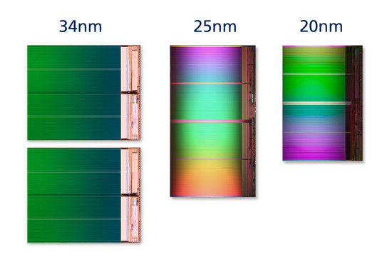
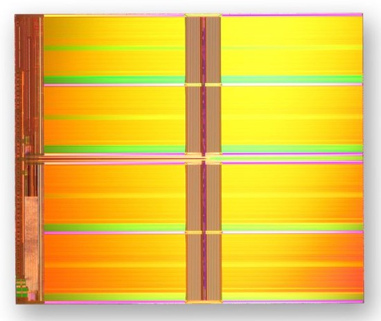
Intel Micron Flash Technologies has announces the next generation NAND circuit, namely a 128 Gb MLC circuit built on 20nm technology. Besides offering record capacity and a new manufacturing technology it sports the fast ONFI 3 interface.
IMFT (Intel Micron Flash Technologies) eaelier announced the world’s first NAND circuit built with 20nm grade technology, in that case a 64 Gb circuits (8 GB) with 2-bit cells (also known as MLC) that use the common ONFI 2.x interface that is limited to bandwidths up to 200 MB/s. The new circuit uncovered by IMFT is the next generation storage memory since it both sports a new ONFI interface, but also much better capacity than any previous NAND circuit.
The new circuits builds on 20nm technology developed together by Intel and Micron, and has a capacity at 128 Gb (16 GB) with 2-bit-cells and the new ONFI 3 interface. The new interface raise the roof for the speed in a circuit/capsule in a SSD or any other kind of memory device. The theoretic max of ONFI 2.x at 200 MB/s is doubled to 400 MB/s. This will lead to cheaper SSDs that can use fewer circuits, and in theory it needs half as many circuits to reach the same capacity as last generation drives, without performance taking a hit. It is all about the maximal bandwidth between the controller and the NAND memory.
 IMFT sports the highest capacity of a NAND circuit
And 128 Gb is also a new record. Considering the capacity it is the largest monolithic NAND circuit so far. You could pair only eight of these in a capsule to get 128 GB of storage. You would then need only eight of these capsules to make a SSD at 1 TB, or sixteen for a 2 TB SSD. Also smaller units like smartphones can make use of this, not the least Ultrabooks and MacBook Air that use minimal SSDs.
While the technology looks good, it while take a while. There are no controll circiuts today that support ONFI 3. Intel and Micron estimates that the first units using the 128 Gb 20nm MLC circuit will be among consumers in 2013. Its 64 Gb 20nm MLC circuit with the older ONFI 2.x interface will go inte mass production and is with partners for validation. The first SSDs based on 20nm technology will be in stores in the middle of 2012.

The biggest question is of course what kind of durability that IMFT has achieved with its 20nm technology? The new technology uses HKMG to maintain a high level of endurance, and to be able to shrink the transistors to this level. IMFT has specified all 20nm circuits to the same 3000 – 5000 write cycles, which is identical to its 25nm technology. We expect 20nm circuit to be cheaper though.


