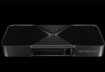
NVIDIA has now finally launched its new video card series based on the new 90nm manufacturing process where the new flagship GeForce 7900 GTX is the main attraction. The G71 architecture is the developing name for the new series (G73 for 7600) and it is more or less identical to NVIDIA’s last G70 architecture, i.e. 24 pipelines and not 32 that some rumors stated. GeForce 7900 GTX has therefore no advantage over the earlier top of the line GeForce 7800 GTX 512MB, bu the new 90nm manufacturing process is the key to GeForce 7900 GTX improved performance. The new flagship has its graphics circuit clocked at 650MHz, which is identical to ATI’s top of the line Radeon X1900 XTX.
GeForce 7900 GTX has been stripped of a number of transistors though and gets around with only 278 million while Radeon X1900 XTX weighs in at incredible 384 million transistors. This makes 7900 GTX a very attractive circuit that is even cheaper to manufacture, even more of a contrast to the GeForce 7800 GTX 512MB. Overall NVIDIA has gone for efficiency and performance/penny, which wasn’t really expected considering the last generation of extreme graphics circuitsfrom both ATI and NVIDIA.
We at NH are working hard on our own preview of the GeForce 7900 GTX where we will take a closer look at how it stands up to its predecessor, 7800 GTX 512MB and ATI’s new Radeon X1900 series. Not only single cards but of course also SLI and Crossfire configurations. Unfortunately we’ve run into som problems with our test system and despite that the article is more or less ready we want to solve these problems first to be able to serve you first class material. You will find out why NVIDIA has chosen this path and how the future looks like with SLI and Quad SLI, don’t worry we have something big coming!
Until then you can take a look at the other previews that have surfaced during the day;
:: Anandtech :: Tech Report :: Hexus :: HardOCP :: Firingsquad ::


