


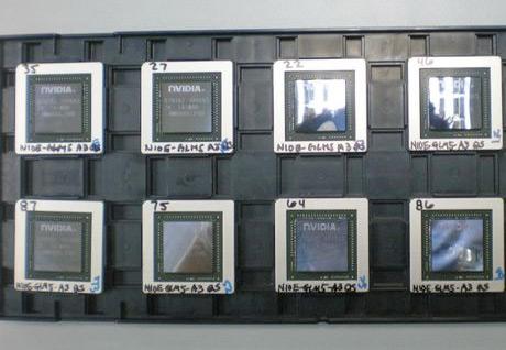
With 3 billion transistors we knew that GF100 would be an extremely big and advanced circuit. It looks like we have some pretty solid information on the size of the die as a user at the Chinese forum NGA has published pictures of the GF100 GPU used by GeForce GTX 470 and GeForce GTX 480.
By examining the photos users have been able to estimate the size of NVIDIA’s GF100 GPU to 23x23mm, which adds up to a total area of 529 mm2, which is significantly larger than the 334 mm2 of AMD’s Cypress GPUs.
That NVIDIA will be having problems with the yields and heat production is something we’ve feared for a long time, and having the huge size confirmed certainly doesn’t leave us feeling better than before. In just a few weeks we will know more.


Leave a Reply