


GeForce GTX 580 will most likely be the most powerful single-GPU graphcis card on the market in 2010. Now that we have the complete specifications for NVIDIA’s GF110 GPU it becomes clear that NVIDIA is attempting to do what it failed to with GTX 480 – going all in – to win the performance war against AMD.
While AMD is working on optimizing the Northern Islands architecture that beside better performance also brings new features, NVIDIA has an own agenda. To prepare its Fermi architecture for a new power struggle to maintain its position as the maker of the world’s fastest snabbaste single-GPU graohics card. A big PR bonus NVIDIA has been able to use over the last six months.
If the increase in frequency and the so far unconfirmed information we’ve come across NVIDIA’s work will result in a graphics card called GeForce GTX 580 that biuilds on a new optimized circuit called GF110. In this post we will try to summarize the information that we have so far and speculate in what this could mean for NVIDIA and the graphics market.
NVIDIA shift focus from server to gaming
The roots of GF100 – the GPU found in GeForce GTX 480 – are clear and the biggest difference is that NVIDIA has revised its priorities since the launch of the original Fermi architecture. The focus is now on retail and games, not companies and servers.
When we posted our first article on NVIDIA’s Fermi architecture in 2009 it was with information on the server performance and features of the architecture. Something that worried us a it since this was the only information NVIDIA wanted to release;
When GeForce GTX 480 eventually launched it turned out that NVIDIA had managed to build a product that worked well in the retail segment too. Tough the graphics circuit was big, hot and consumed power like none other.
To get the card out on the market NVIDIA was forced to cut corners, wjere the perhaps most obvious was that it had to deactivate one of its sixteen streaming multiprocessor clusters, which reducsed the number of active CUDA cores to 480 instead of 512 that the circuit was designed to use.
NVIDIA makes full use of Fermi
Fast forward six monther and here we are and are on the road to seeing the first Fermi GPU that gets to use all 512 CUDA cores at its disposal. By activating all 16 SM units GTX 580 will also gain access to more texture units and ROPs.

NVIDIA has revised the Fermi family cooler before the GTX 580 launch
This has been one of the most important pieces in the development of GeForce GTX 580, that like its precursor had to sacrifice other functionality to reach the final goal.
GF110 focuses on retail, without HPC functions
We have had a hard time seeing how NVIDIA would be able to activate its sixteenth SM unit without severe problems with the power consumption. But with GF110 NVIDIA made an active choice and sacrificed the HPC functionality (High Performance Computing) that it talked so boldly about for Fermi, not only to make it smaller but also more efficient.
According to sources to NordicHardware it can be as many as 300 million transistors that NVIDIA has been able to cut in this way. The effect is that GF110 will be a GPU targetting only retail and will not be as efficient for GPGPU applications as the older siblings of the Fermi Tesla family. Something few users will care about.
| GeForce GTX 580 | GeForce GTX 480 | |
| Graphics circuit |
GF110 |
GF100 |
| Node | 40nm | 40nm |
| CUDA cores |
512 st. | 480 st. |
| GPU clock frequency |
775 MHz | 700 MHz |
| CUDA clock frequency |
1 544 MHz | 1 400 MHz |
| Memory clock frequency |
4 008 MHz | 3 696 MHz |
| Memory interface |
384-bit | 384-bit |
| Memory buffer |
1 536 MB | 1 536 MB |
| Memory bandwidth |
192,4 GB/s | 177,4 GB/s |
| Texture fillrate | 49,4 GTexel/s | 42,0 GTexel/s |
The latest information that has reached us are said to be the final specifications for NVIDIA GeForce GTX 580. These were published at it168.com and strengthen the information we received earlier. There we can clearly see how NVIDIA beside processing units also raised the clock frequencies for both memory and GPU. This was made possible through a more mature circuit manufacturing where NVIDIA has managed to lower power consumption of GF100 with 10-15% without any physical alterations. This gave the comany more margin to work with.
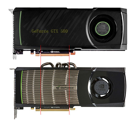
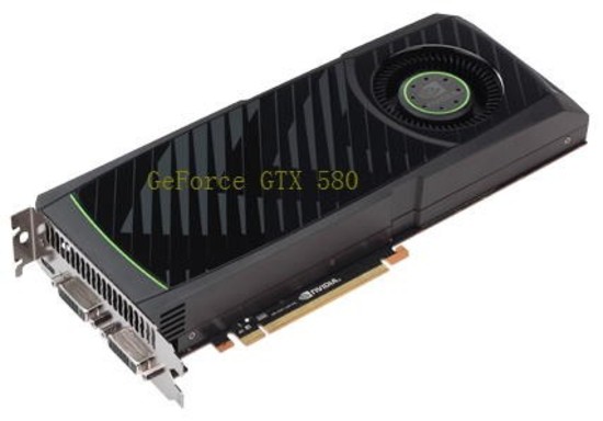
GF110 is pin-compatible with GF100 and will thus be similar physically
According to our sources the higher clock frequencies and the increased number of CUDA cores enable NVIDIA not just to increase performance compared to its own flagship, but also be enough to keep AMD Radeon HD 6970 in second place.
Even if the launch date hasn’t been set yet, it looks like November 20th is the hottest candidate, which is about the same time we expect the Radeon HD 6900 series.
Neither NVIDIA nor AMD confirms any of the information we have posted today and even if changes may happen we are starting to get a pretty good picture of what we can expect from the graphics industry this Winter. NVIDIA and AMD looks to continue its fight where both parties are sticking to their original plans, AMD working on its less advanced but more efficient circuits while NVIDIA focuses on raw strength.
Source: Our own, it168.com, PCinlife.com


Leave a Reply