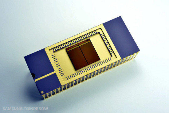
Samsung is one of the leading manufacturers of flash memory, something it has further enforced now that it will start mass production of V-NAND, or Vertical NAND, where the memory circuits can be stacked vertically for 128 gigabit, or 16 gigabyte, per chip.
Earlier today we reported on the potential competing memory technology RRAM from Crossbar that could scale through stacking inside the memory capsule. Stacking circuits is not new, but for flash storage it has been surprisingly hard to achieve in large retail production.
Samsung has now started mass producing Vertical NAND, or V-NAND. The technology allows for up to 24 memory cells to be stacked inside a memory chip for a total of 128 gigabit per chip. For retail consumers that means 16 gigabyte per chip. This is on par with TLC-NAND that is currently being used by the 840 Evo-SSD, but with higher scalability.

It also points out that the technology will lead to 2 to 10 times better reliability over traditional NAND-flash and double the write performance. The scalability will double with the extra dimension that is added to the construction process, which will be one of the most important properties when flash makers start to fight the drawbacks of the aggressive node jumping.
Samsung says the technology lays the ground work for getting closer to chips with 1 terabit capacity in the future, I.e. 128 gigabyte per module. This means storage in the terabyte range in mobile phones is not that far off as we take on new process nodes in the future.
Exactly when the technology will become commercially available is unclear, but judging from previous flash technology launches it could be before the end of the year, but could take until next year sometime.
Source: Samsung


