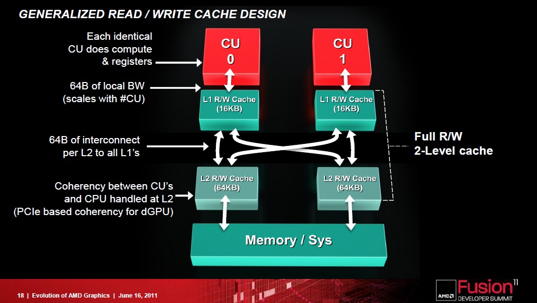
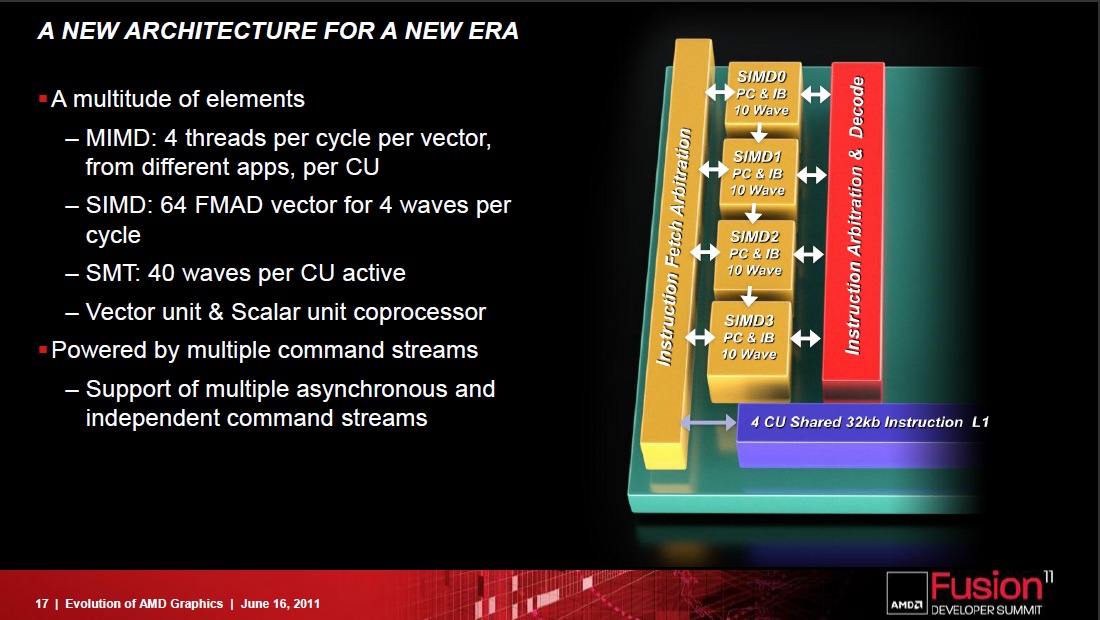
AMD’s new architecture Southern Islands is expected to launch later this year and will be the first on the new 28nm process. AMD has, during the Fusion Developer Summit, revealed new details on what will come, and Southern Islands will not be a refining of the Cayman GPU found in the HD6900 series, but something completely new with real cache structure and no more VLIW.
AMD surprised with the launch of HD 6970 an dCayman GPU that had fewer stream processors than the previous flagship HD 5870, but still performed better thanks to a small but significant change in the architecture. Southern Islands will not, contrary to earlier rumors, be just a refurbished version of Cayman, but all new design from the bottom and up. AMD has more or less used the base design from the launch HD 2900XT for 4 years ago.
 It throws out the VLIW design and replace it with what it calls a Compute Unit. The new units will sport several elements from different design concepts, like being able to execute a larger number of instructions and a MIMD design; Multiple Instruction stream, Multiple Data stream. Simultaneous Multi-Threading (SMT) is available in the architecture and many will recognize this from Intel’s processors where it has enabled eached core to handle 2 threads, also known as HyperThreading. It has also implemented a genuine cache structure, something NVIDIA has used for a long time.
Its VLIW design offers really high FLOPS if you compare HD 6970 to GTX 580, AMD’s alternative is almost twice as capable with 2.7 TeraFLOP, but in most cases GTX 580 wins in parallel calculations where GPGPU triumphs. The reason for this is a design that is much simpler to program for, but also NVIDIA’s own programming language CUDA. What AMD does with its Compute Unit is to make this bit a lot batter and simpler to work with for developers, which has complained for long about how hard it is to program for AMD’s GPUs.
 Fusion is all about getting the most of both worlds
Another big news is that architecture will support x86-64 memory addressing, which will make it possible for both CPU ang GPU to share memory. This will make it faster to load new textures in games and allow developers to get access to “really virtualized memory” according to AMD.
The new support for memory addressing will come to great use with its coming APUs. Llano and Ontario acts just like before when it comes to memory where it has to address a certain portion (128 MB, 256 MB, 512 MB etc.) in BIOS for the GPU and thus lose a bit of the memory regularly available to the processor. Instead both CPU and GPU can share all of the memory in the system or use it all when needed.
The new architecture also has full support for C, C++ and other high leverl languages to make it even easier for developers to use the power of the GPU and the list of support programming languages will grow with every generation says AMD.
Source: PCPerspective


