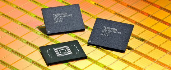
Only days after Intel and Micron proudly announced its 20nm process for NAND flash memory competitor Toshiba has announced it has come one step longer. Toshiba says it has started test manufacturing NAND flash circuits with 19nm technology, circuits that will be ready for mass production in Q3 2011.
Toshiba took a big hit with its NAND flash manufacturing with the earthquake in Japan, but looks to be in surprisingly good shape. The company is said to have cut the number of shipped NAND flash circuits in May and June in half due to material shortage after the quake, but it is now moving toward making its first Multi-Level Cell NAND chips at 19nm. The MLC chipset have a density of 64Gb (8GB) and will according to Toshiba be the smallest in the world with a surface of 118mm2, which could double the capacity in mobile devices or storage products.
The new 19nm chips use Toggle DDR2.0 technology for better performance. At the same time the chips will scale to a 3-bit per cell design, which would increase density by 50%.

Current mobile phones ships with 32Gb at most, normally. With Toshiba’s new circuits this could be moved up to 128GB without problems. This isn’t just an alterantive for cost efficient reasons, but also shows what the new NAND flash circuits are capable of.
Mass production is expected to start in Q3, while IMFT (Intel Micron) is said to start production of 20nm NAND circuits in Q2 2011.


