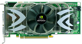
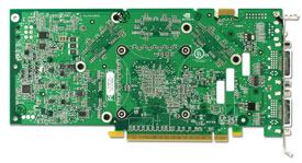
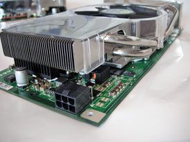
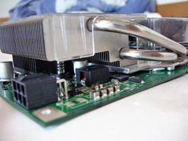
We’ve taken a closer look at NVIDIA’s new flagship GeForce 7900 GTX. How does its compare to its predecessor and today’s king of the hill from ATI, Radeon X1900 XTX?
NVIDIA and ATI are probably clashing together in one of the toughest and hardest competitions we’ve seen on the graphics market. Since the first rumors about ATI’s R520 circuit and the peak when R520 finally arrived NVIDIA and ATI haven’t given an inch to each other. The last couple of months have been eventful the least to say starting with ATI releasing its R520, which was countered by NVIDIA’s GeForce 7800 GTX 512MB, it was now ATI’s turn to counter with Radeon X1900 XTX. So now it’s NVIDIA’s turn to respond with their alternative to ATI’s X1900 series.
NVIDIA has chonse to respond to ATI by releasing new graphics circuits based on their G70 architecture. It’s not a big surprise that little has happened since the G70 and the GeForce 7 series considering NVIDIA’s developing name G71. The architecture is actually pretty much identical to its predecessor. Despite this there are actually many interesting things to say about NVIDIA’s new circuits, the most obvious being NVIDIA’s decision to use a 90mm manufacturing process for its high performance circuits. The GeForce 7800 series used a 110mm manufacturing process that had limitations with both frequencies and higher heat dissipations.
On March the 9th NVIDIA released no less then three different video cards, GeForce 7900 GTX, GeForce 7900 GT and the GeForce 7600 GT. In today’s review we’re going to focus on the flagship GeForce 7900 GTX , the most interesting technologically speaking. Quite simply how NVIDIA has managed to push the limits further on the video card market. We will soon also deliver a more thorough review of GeForce 7900 GT and 7600 GT, which are both two very interesting cards so don’t worry, we haven’t forgotten.
But right now we’re going to take a closer look at the notorious GeForce 7900 GTX and since this is a extreme card for extreme users we are going to put it through some extreme situations. You can expect the usual performance tests but to top it off we’ll also be doing some extreme performance tests later on.
Let’s take a closer look at the GeForce 7900 GTX and one of the most persistent rumor about the G71, the one that claims that the circuit would use 32 pipelines, a rumour that has proved to be false.
One of the first rumors that arose about the G71 architecture was that NVIDIA would take one step further in amount of pixel pipelines their video cards were using. They increased from 16 pipelines in the NV40 series (GeForce 6800) to the full use of 24 pipelines in the G70 series (GeForce 7800 GTX). When you think of the huge success the GeForce 7 series were, not only in amount of performance but also in power consumption and heat dissipation, it seemed like NVIDIA were on the right track.
ATI’s R520 architecture that were, for ATI, regrettably delayed was
also rumored as a 32 pipeline architecture. But when the chip came ATI didn’t
want to say anything about a certain number of pipelines but more about the
amount of execute units inside the chip. The R520 (X1800 XT)
was a 16 pipeline architecture and ATI showed seriousness by ignoring the
amount of pipelines even when they introduced the R580 (Radeon X190XTX) with a
16 pipeline architecture. Then it was the amount of pixel shader units in the
pipeline that had been increased from 16 units on the R520 to the amount of 48
units on the R580. This means more performance within the
pipelines.

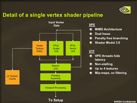
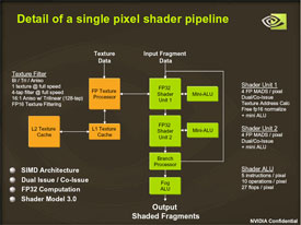
Diagram over the G70/G71 architecture
When NVIDIA introduced GeForce 7800 GTX 512MB it was made clear that money and production cost does not have to be a obstacle to introduce a new high-end video card. NVIDIA’s GeForce7800GTX 512MB knocked ATI’s Radeon X1800 XT and even though it cost a fortune it sold well. In other words NVIDIA showed that there were a lot of enthusiasts willing to pay the prize for top performance. A fact that made the rumors of a 32 pipeline architecture even stronger when the cost probably would be NVIDIA’s biggest problem.
NVIDIA chose not to go further than 24 pipelines for the G71 architecture
and the reasons are several and coincide pretty well with the speculations we have shown here at NH earlier. NVIDIA
could have released the G71 with a 32 pipeline architecture, but the
price would be higher. Although success with the 7800 GTX 512MB
NVIDIA was not interested in releasing a video card with a price tag near
$750, at least not for a new product series. NVIDIA have more or less made a
U-turn with the G71 if we look at the trend they seemed to create with
their release of 7800 GTX 512MB and we will take a closer look on that
later.
Even if GeForce 7900 GTX "only" is a 24 pipeline architecture like its
predecessor NVIDIA mean that they don’t abandon a concept with more pipelines.
To the question why NVIDIA chose not to use more pipelines NVIDIA’s
CEO/President answered;
”You asked for more pipelines, we now offer you 96 – Quadro
SLI”
We got this spoken answer when we were at NVIDIA’s headquarters in Silicon
Valley where questions about the G71 architecture had been on the agenda
several times during the introduction of the new architecture. The result is
that NVIDIA goes for cheaper single card and those seeking extreme
performance can aim for multiple cards. Here the price tag of the 7900
GTX plays a significant role, which showed to be a totally different story than we were
prepared for after the release of GeForce 7800 GTX 512MB.
Perhaps now you wonder how NVIDIA could match and exceed the performance of
the G71 architecture with the same basic condition, the answer is simple and
logic. By using a more advance and effective manufacturing technology it
is possible to increase the clock frequency inside the graphics processing unit
without problems with heat dissipation and power consumption. It shows that
NVIDIA have gone further than that in ots advance to 90nm, all for better efficiency.
To ask why NVIDIA has gone over to 90nm manufacturing process is like when you buy new pair of tennis shoes cause the old ones are worn out. It’s simply a part of development when you’ve stressed out the old manufacturing process to the limit, you introduce a new and refined process to progress. Seen this way NVIDIA’s transfer to 90nm is expected. There are a few fundamental rules that a new manufacturing process brings along with it;
:: Smaller transistors and lower voltage which gives lower power consumption and heat development
:: The possibility to raise the frequencies without the increase in power consumption compared to earlier manufacturing process.
::
Smaller core which adds to more cost efficient manufacturing (more yield per wafer)
The first two things are closely related when you put into perspective that the chip can work at a lower voltage and develop less heat to push the frequencies even higher and still have similar power consumption and heat development as earlier generations, which generates into free performance.
NVIDIA managed to refine the manufacturing of the G71-core when they went over to the 90nm manufacturing process, they’ve also looked at the construction of the core and without altering its function and features they’ve managed to trim the construction by doing away with a couple of million transistors which along with the smaller manufacturing process given a core which is significantly smaller than the core of the GeForce 7800 series. Below we’ve compared NVIDIA’s 110nm GeForce 7800 series against the new 90nm GeForce 7900 series to see what NVIDIA’s work with transistor count and manufacturing process has done for the video cards core, we’ve also thrown in a ATI Radeon X1900 for comparison.
| GeForce 7900 | GeForce 7800 | Radeon X1900 | |
| Codename: | G71 | G71 | R580 |
| Manufacturing process: | 90nm | 110nm | 90nm |
| Transistor count: | 278 million | 302 million | 384 million |
| Core size: | 194mm² | 334mm² | 315mm² |
NVIDIA had not surprisingly a pretty big core on the 7800 series which compared to ATI’s Radeon X1900 series suffered from its 110nm manufacturing process. Now when NVIDIA not only have done away with 24 million "useless" transistors and also switched manufacturing processes the tables have been turned. The GeForce 7900 series a very small core if compared to earlier video cards in the same genre. The core of the GeForce 7900 is a whopping 72% smaller than the core of the GeForce 7800 and that is very interesting for NVIDIA’s production costs. On a 300mm wafer you can now fit 70% more cores of the 7900 architecture compared to that of the GeForce 7800, simple mathematics tells us this gives an enormous profit in the production cost. You also see that ATI is likely to have a significantly higher production cost with their relatively large X1900 core.
NVIDIA’s progress with the manufacturing process and they’ve chosen to stick with their original 24 pipeline architecture have resulted in a truly cost efficient solution and be live it or not, but now "most bang for the buck" is one of NVIDIA’s slogans, just as most performance/watt was when the GeForce 7800 series were introduced. This is to say the least a pretty remarkable turn for a company who just a few months ago introduced one of the most expensive and powerful video cards targeted to the ordinary consumer.
The introduction price for the Geforce 7900 GTX is $499 for distributors which can be compared to $649 which was the guideline price for the GeForce 7800 GTX 512MB when it was introduced. And also the GeForce 7900 GT will get a very competitive price compared to its competitors on the market and we’ll look closer at that fact in a future article. NVIDIA has probably thought along the lines of, if ATI will continue to want the most powerful video card they wont make any money of it. Not surprisingly ATI announced that they will lower the price on all their RAdeon X1000 based video cars to be price competitive
NVIDIA has not closed the door completely for future monsters with a similar frightening price tag as the GeForce 7800 GTX 512MB. When NVIDIA representatives were asked about the possibility of a GeForce 7900 GTX 1024MB model or something similar to the 7800 series 512MB GTX card we were met with smiles and the standard phrase;
"We cannot comment on non-introduced products"
With all honesty though NVIDIA hasn’t loosened its grip about the performance throne with the launch of of the GeForce 7900 series. Even if they’ve seem to have become "nice" with their flagship 7900 GTX NVIDIA’s CEO Jen-Hsun Huang delivered an answer for those who want more and at the same time makes NVIDIA’s claim to be performance leading on the video card market with ease. Namely NVIDIA’s multi-GPU technique SLI and introduced with the GeForce 7900 series, Quad SLI!
NVIDIA has for one and a half year had its multi GPU technology SLI as an ace up its sleeve, and even though it wasn’t exactly lacking problems in the beginning, it has matured significantly during the last year. Especially after launching its GeForce 7800 series. To make a short resume, SLI works by connecting two video cards together in a computer and then with the right software work together in rendering heavy graphics. The theoretical gain in performance could be considered to be 100%, but there are certain bottlenecks that drag down the efficiency of the technology. But performance gains of over 80% with two video cards in SLI is nothing unusual with the right applications.
Even if few consumers has money to spend on SLI systems, the technology has done some great PR for NVIDIA, as they all along has been able to brag about them having the fastest performing graphics rendering system, even though ATI had the fastest individual card.
SLI continues to be an important asset for NVIDIA and during the launch of their 90nm video card series, they’ve focused much on this. As they’ve pushed the prices on their flagship 7900 GTX and at the same time launch 7900 GT they at the same time opens the door for those who has been considering an SLI system, but have felt that the pricing has been a big block. It’s still far from cheap to buy an SLI system, but NVIDIA wants it to be a clear option for those who feel that one video card just won’t cut it. Instead of buying one graphics card for $750, you could buy two for $1000 that gives way more options, but still better performance.
NVIDIA has thanks to the 90nm technology and optimized manufacturing process managed to keep the power consumption to a really respectable level. But if you are about to use an SLI system, you still need a whole lot of juice. These guidelines NVIDIA have set for their "SLI classes" to make it clear which kinds of power supplies are required.
|
Ultra High-End SLI PC: |
High-End SLI PC: |
| Ultra High-End NVIDIA SLI Configuration: -Dual GeForce 7900 GTX 512MB or Dual GeForce 7800 GTX 512MB -AMD Athlon 64 FX-60 2.6 GHz or Intel Pentium EE 955 3.46 GHz -NVIDIA nForce4 SLI X16 motherboard with 2GB RAM -Twp harddrives using Raid 0 -Two optical units -PCI sound card -LCD at 1600×1200 resolution |
High-End NVIDIA SLI Configuration: -Dual GeForce 7800 GTX 256MB or Dual GeForce 6800 Ultra -AMD Athlon 64 FX-57 2.8 GHz or Intel Pentium EE 840 3.2 GHz -NVIDIA nForce4 SLI X16 motherboard with 2GB RAM -Two harddrives using Raid 0 -Two optical units -PCI sound card -LCD at 1600×1200 resolution |
|
Mid-Range SLI PC: |
Low-End SLI PC: |
| Mid-Range NVIDIA SLI Configuration: -Dual GeForce 7900 GT or Dual GeForce 6800 GT or Dual GeForce 6800 -AMD Athlon 64 4000+ -NVIDIA nForce4 SLI motherboard with 1GB RAM -One harddrive -Twp optical units -PCI sound card |
Entry-Level NVIDIA SLI Configuration: -Dual GeForce 7600GT or Dual GeForce 6600 GT or Dual GeForce 6600 -AMD Athlon 64 4000+ -NVIDIA nForce4 SLI motherboard with 1GB RAM -One harddrive -One optical unit |
Without a doubt, a whole lot of power is required from the PSU in an SLI system, and it will be interesting to follow the market for video card power supplies which seems to get started at CeBIT.
SLI is as earlier mentioned, a really important asset for NVIDIA and their video card development, but they aren’t any longer alone with a multi GPU solution. ATI launched a few months ago their answer to NVIDIA’s SLI technology, ATI Crossfire. Crossfire is just as SLI pretty packed with small problems, but since the ATI’s launch of the RD580 (Crossfire Xpress 3200) chipset it has became a more matured solution. In other words a great opportunity for NVIDIA to yet again raise the stakes for multi GPU systems by launching a further developed version of SLI that supports a full four video cards in the same system, Quad SLI.
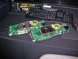
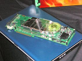
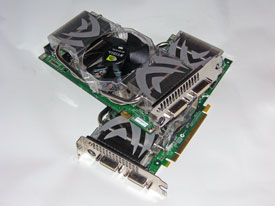
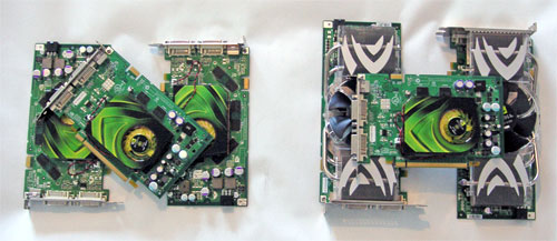
SLI has been considered a technology only for the wealthy and fortunate by many. Perhaps not far from the truth, but with Quad SLI NVIDIA has really managed to make this clear. There isn’t much to say about Quad SLI technically more than that SLI software has been developed to divide the workload over four graphics circuits instead. When it comes to the hardware Quad SLI is a bit different from the regular SLI technology. We’ve heard rumors that ASUS used two ASUS EN7800GT Dual video cards to test Quad SLI and NVIDIA has chosen the same path. It will not make Quad SLI possible by using four regular cards in an SLI configuration but NVIDIA will instead launch specially made dual-cards with two graphics circuits integrated on the same card. Two of these can then be used with a regular SLI motherboard to create a Quad SLI setup.
Quad SLI is launched today for OEM use and will be available through prebuilt systems from various PC builders around the globe. Except for large international PC builders such as Dell, there will be nation exclusive offers. E.g. we now that online computer store Komplett will offer Quad SLI systems in the future and considering the small group of people NVIDIA is targeting availability shouldn’t be a problem. First of all a Quad SLI system will cost a fortune, exactly how much depends on the system builder’s choice of components. But except for the computer NVIDIA recommend that you invest in a extremely high resolution monitor to really make use of the power available with Quad SLI. They’ve chosen to present Quad SLI with a Dell 3007W, Dell’s new 30″ LCD monitor with a resolution at 2560x1600px and cost $2,199. Quad SLI will appear on the retail market, but not until the end of March. No matter how you twist and turn the cost for Quad SLI will be hugh, especially if you want to use it to the fullest.
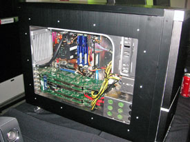
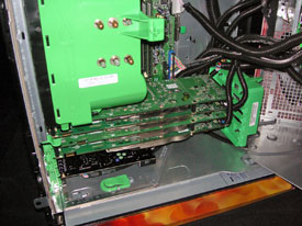
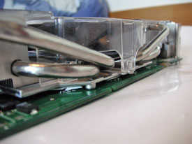
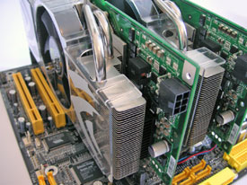
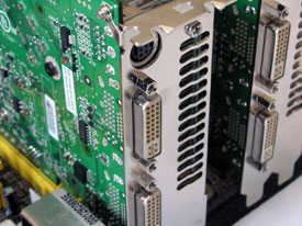
NVIDIA doesn’t supply any test systems for Quad SLI but lets this responsibility lie on its OEM partners and we haven’t received any more detailed information about the card that will be used, but we managed to take some pictures of a Quad SLI system during our stay at NVIDIA’s headquarter and we also have some specifications for the 7900 Dual card that will be used with these systems.
|
Specifications – NVIDIA 7900 Dual
|
|
| Developing name : | G71 |
| Manufacturing process: | 90nm |
| Transistors: | 2 x 278 million |
| Pixel shader processors (pipelines) | 2 x 24 (48x, 96x Quad SLI) |
| Vertex shaders | 2 x 8 (16xt, 32x Quad SLI |
| ROPs: | 2 x 16 (24x, 48x Quad SLI) |
| GPU frequency: | 2 x 500MHz |
| Memory controller : | 256-bit to memory |
| Memory support: | 256-bit, 600 MHz GDDR3 (1200MHz) |
| Memory amount: | 1GB (2GB Quad SLI) |
| Fillrate: | 15.6 billion |
| Memory bandwidth : | 2 x 38.4GB/s (total 153.6GB/s in Quad SLI) |
| Standard outputs: | 2x Dual-link DVI |
Quad SLI is without a doubt a majestic dream to 99% of all computer enthusiasts, but NVIDIA has shown that it has the technology and the knowledge to conquer such a task, such a extreme graphics system as Quad SLI. We here at NH will of course take a closer look at Quad SLI and hopefully in a near future be able to offer you performance tests and other such delights. It is going to be especially interesting to see how much difference the lower clocked circuit the Quad SLI card uses will make. Both GPU and memory are considerably lower clocked than we had expected when we look at GeForce 7900 GTX, which is because NVIDIA has certain power consumption demands it didn’t want to breach, and at the same time the cooling would have become a major issue.
That’s all we have to say about Quad SLI for now , soon we will venture on and test NVIDIA’s new flagship in both single and SLI configurations, but first lets have a look at the card.
As we’ve only had the card for a very short period of time we’ve chosen to focus on NVIDIA’s new flagship GeForce 7900 GTX with today’s review and the goal with this card is simply to reclaim the performance throne from ATI and its Radeon X1900 XTX. We have already stated that NVIDIA hasn’t modified the architecture much more than tune the 90nm manufacturing process. But what is the result of this transistor shrinkage and what are the specifications for 7900 GTX?
 |
|
| Developing name: | G71 |
| Manufacturing process : | 90nm |
| Transistors: | 278 million |
| Die size : | 194mm² |
| Pixel shaders (pipelines) | 24 |
| Vertex shaders | 8 |
| ROPs | 16 |
| GPU frequency(MHz): | 650 (700 Vertex) |
| Pixel fillrate (Billion/sec): | 10.4 |
| Texel fillrate (Billion/sec): | 15.6 |
| Memory interface : | 256-bit |
| Memory amount : | 512MB |
| Memory frequency (MHz): | 800/1600 |
| Memory bandwidth (GB/s) | 51.2 |
| RAMDAC: | 400MHz |
| Cooling system : | Double slots |
| Standard outputs: | 2x Dual-link DVI, 1x S-video |
| Price: | $499 |
The fact that NVIDIA has chosen to use the same base architecture with the 7900 series as the 7800 series makes most specifications match with the previous high end card from NVIDIA: GeForce 7800 GTX 512MB. But there are details that have changed and these are the frequencies, both GPU and memory. GeForce 7900 GTX has thanks to its optimized 90nm manufacturing process received a processor frequency at 650MHz, the same as ATI’s graphics circuit with Radeon X1900 XTX. If you compare to NVIDIA’s 7800 series the difference is huge. GeForce 7800 GTX has an almost pathetic clock at 430MHz while the handpicked GeForce 7800 GTX 512MB could proudly march on at at 550MHz, which is still 100MHz less than 7900 GTX.
Worth mentioning is that NVIDIA has with GeForce 7900 GTX once again chosen to use different frequencies for the core itself and the vertex units. With 7800 GTX the core worked at 430MHz while the vertex units worked at 470MHz. With 7900 GTX the equivalent numbers are 650MHz core and 700MHz with the vertex units.
The second thing it has changed is the memory speed which is now at 800MHz (1600MHz DDR), a tiny bit slower than GeForce 7800 GTX 512MN, that had its GDDR3 memory clocked at 850MHz (1700MHz DDR). Still considerably higher than what 7800 GTX could show off, the memory with this card was clocked at only 600MHz (1200MHz DDR).
We’ve earlier taken a peak at GeForce 7900 GTX’s memory chips and they seem to be the same model as the one 7800 GTX 512MB had, namely Samsung’s 1.1ns GDDR3 chip, specified for 910MHz (1820MHz DDR). NVIDIA has chosen the "better-safe.than-sorry"-path here.
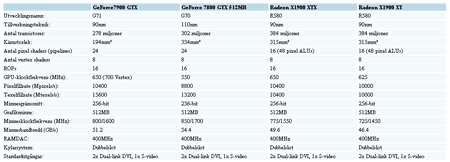
To give you en overview of GeForce 7900 GTX’s specifications compared to other high performance cards of today we’ve compiled this table.
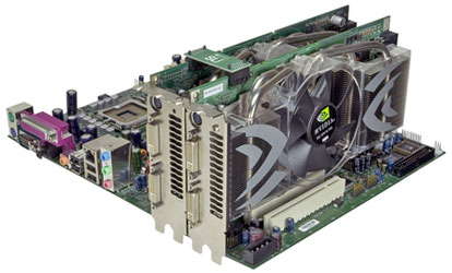
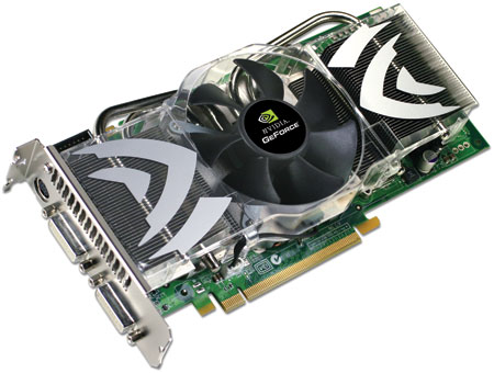
Here we see some pictures of NVIDIA’s new flagship and in our coming article about extreme overclocking we will not only check out how the card looks like without the cooler but also show you how to do a voltmod to reach even better results. Now the time has come for the regular performance tests though and we start, as usual with the test system and the tests.
Test system |
|
 | |
|
Hardware
| |
| Motherboard | DFI NF4 SLI-DR Expert (FX-60 bios) |
| Processor | AMD Athlon FX-60 (Toledo, 0536SPMW) |
| Memory | Corsair XMS3200LL rev1.1 2x512MB (BH-5) |
| Harddrive | WD Raptor 36GB 10 000 RPM |
| Monitor | Dell UltraSharp 2405FPW |
| Video cards | NVIDIA GeForce 7900GTX NVIDIA GeForce 7800GTX 512MB ATI Radeon X1900XTX ATI Radeon X1900XT Master |
| Power supply | OCZ PowerStream 600W SLI |
|
Software
| |
| Operating system | Windows XP (SP2) |
| Drivers | nForce 6.70 Catalyst 6.3 ForceWare 81.89 |
| Monitoring program | Fraps 2.5.0 |
| Test program | 3DMark2001 (3.3.0) 3DMark03 (3.6.0) 3DMark05 (1.2.0) Battlefield 2 World Of Warcraft Call of Duty 2 – Demo Doom 3 (1.0.1262) Far Cry (1.32) Half-Life 2 Need For Speed Underground 2 Unreal Tournament 2004 (v3399) |
GeForce 7900 GTX is a high performance card all the way through and the fact that we’ve chosen to wait with presenting NVIDIA’s mid-range (7900 GT) and budget class (7600 GT) cards has made it possible for us to focus solely on the market’s true beasts with this review. Performance tests with mid range and budget cards will come soon though.
The perfect opponent for GeForce 7900 GTX is of course ATI Radeon X1900 XTX and how these cards stand up to each other is of course one of the main parts of our tests, which cards will come out on top from this glorious fight? We will of course not just use the cards one by one, but both of NVIDIA’s and ATI’s video cards gets to show what it can do in multi GPU configurations, SLI vs Crossfire.
Except from this given comparison with NVIDIA and ATI’s honor at stake, we have another very interesting comparison we will return to later in our tests. Namely the one between GeForce 7900 GTX and NVIDIA’s monster GeForce 7800 GTX 512MB. The first has the GPU power to its advantage thanks to the higher frequencies the 90nm technology makes possible, while 7800 GTX 512MB actually has more memory bandwidth. With other than that identical base architecture this is a truly interesting test.
Before we move on to the performance tests we will take a look at under what circumstances we’ve chosen to test the cards here. The goal was to test all games with with three different resolutions, 1280×1024, 1600×1200 and 1920×1200. The two first are more less classical resolutions for high performance cards, due to the inheritance from the CRT monitors. The last is the standard resolution for larger widescreen LCD monitors, 23″-24″, which is becoming more and more common with high performance computers. These video cards should be able to handle these high resolutions and as you will see they also do, alas the game developers are not as eager to implement widescreen support as one would think. Which means we’re unable to give you performance tests with 1920×1200 with all games, with some games you can work around this but we did not have the time to do so here.
Other than that all tests are done with (3Dmark the exception) 4x antialiasing and 16x anisotropic filtering, graphic setting that will result in better performance and that all owners of such cards can afford to use.
Regarding the motherboard, we’ve chosen to use DFI NF4 SLI-DR Expert with NVIDIA’s video cards and ASUS A8R32-MVP Deluxe with ATI’s video cards. Unfortunately we couldn’t use two "true" x16 PCIe lanes as nForce4 SLI only sport 2×8 PCIe. This results in a theoretic difference, but our internal tests shows that the difference is none or at best not even neglible. Although it may be worth mentioning that NVIDIA’s video cards might have a little more to give with the SLI tests. We will also update our performance tests with an nForce4 SLI X16 motherboard soon.
Now its time to present the performance tests to find out what video card is the fastest today.
| Setting: | Value: |
| Resolution | 1024×768 |
You shouldn’t use Futuremark’s 3DMark-series to test how a video card performs in games, because 3Dmark is, quite simply, a graphics demo and not a game. It is however a benchmark that is easy to use and extremely popular amongst enthusiasts. We have performed four tests in 3DMark and the results are fairly scattered. The X1900 XTX gains a minimal victory in the CPU demanding 3DMark 2001, while the 7900 GTX counters with an obvious victory in 3DMark03. The latest two versions of 3DMark yield almost the same performance on both ATI’s and NVIDIA’s flagships, whether we use one or two graphics cards. We have chosen to focus on ATI’s and NVIDIA’s two flagships, but in our coming performance review, we will also include tests from the Radeon X1900 XT and the GeForce 7800 GTX 512MB.
Next, we have the first game tests using Doom3.
| Setting: | Value: |
| Special Effects | Yes |
| Enable Shadows | Yes |
| Enable Specular | Yes |
| Enable Bumpmaps | Yes |
Doom3 is and has always been a strong side for NVIDIA’s video card architecture; the G70 and G71 performs especially well in games based on the Doom3 engine. The Radeon X1900 has problems keeping up when compared to the GeForce 7900 GTX, which raises the bar further compared to the GeForce 7800 GTX 512MB. We see that Doom3 is proof that CrossFire has got excellent potential when it comes to performance, but similar to when NVIDIA’s SLI technology was introduced, most major titles doesn’t support it. However, the support keeps growing every day. In any case, there’s nothing wrong with CrossFire, but unfortunately the architecture of the R580 doesn’t keep up in Doom3. The differences between the video cards are the same, whether we use AA or AF.
We move on with ID Software’s latest title that is based on a finely tuned Doom3 graphics engine.
| Setting: | Value: |
| Special Effects | Yes |
| Enable Shadows | Yes |
| Enable Specular | Yes |
| Enable Bumpmaps | Yes |
Quake 4 is based on a finely tuned version of the Doom3 graphics engine. The results will be more positive for NVIDIA because its architecture suits this engine better. We will soon start using Quake 4 for performance tests instead of Doom3, the results are similar and after its launch,
Quake 4 has kind of replaced Doom3. If you only want to play ID Software’s latest games, you should without a doubt, choose NVIDIA and if possible, its GeForce 7900 GTX. But we presume that most of you want to play other games than Doom3 and Quake 4 and therefore we will continue our tests.
We’ve tested two OpenGL-based games and we will now look closer at our first Direct3D-based game, Call of Duty 2.
| Setting: | Value: |
| Number of Dynamic Lights | High |
| Model Detail | Normal |
| Z Feather Smoke | Everything |
| Number of Corpses | Insane |
As we mentioned earlier we’ve been having some problems with our performance test for this preview and COD2 seems to be one of the biggest troublemakers. Since we only use the COD2 demo we couldn’t use the latest patches and therefore we never got the ATI Crossfire to work, which it does in the full version. We will update the results in our performance-article with both SLI and Crossfire test and we’ll also try with AA turned off and AF turned on.
When using 4xAA and 16xAF it’s an even match between Radeon X1900 XTX and GeForce 7900 GTX, COD2 is a game that demands much of your computer and it clearly shows in the results that show barely playable performance even though we have the best cards on the market to test it with.
Let’s move on to the classic FPS Far Cry.
| Setting: | Value: |
| Texture Quality | Very High |
| Texture Filter Quality | Trilinear |
| Particle Count | Very High |
| Special Effects Quality | Very High |
| Environment Quality | Very High |
| Shadow Quality | Very High |
| Water Quality | Very High |
| Lightning Quality | Very High |
Just like in COD2 we couldn’t get the SLI and Crossfire cards to work and therefore we’ll include those results later.
The results are relatively even and NVIDIA starts by winning a few rounds before ATI squeezes by when we activate AA and AF. When we activated AA and AF in the ATI control panel the performance became considerably worse which is an interesting phenomenon that we have brought up earlier. It’s also worth noticing that our test demo was mostly played indoors but once we got out into open environments the frame rates when through the roof for the ATI card.
We couldn’t find any good explanation for this.
It’s time for our last test, F.E.A.R
| Setting: | Value: |
| Soft Shadows | On |
F.E.A.R is one of the tests that demand much of the video card but despite that both the GeForce 7900 GTX and Radeon X1900 XTX perform well.
Once again it’s a very close fight between the two individual cards while Crossfire is having some problems keeping up to NVIDIA’s SLI technology, this is probably caused by not as good optimizations.
We have already seen in e.g. the Doom3-engine what kind of increase in performance Crossfire can produce.
But if we try to declare a winner it’s hard if not impossible to decide one card.
As most of you may have noticed, he haven’t been able to present as many performance tests as usual in this article and unfortunately the actual benching sessions have been a history of its own. We’ve had to discard several benchmarks due to inexplicable results, and in the results we did publish there are still a few tests that we will continue to investigate. During roughly two straight 30-hour shifts, we’ve run through our test procedures twice, which is why this article is a bit late. We will be reviewing our test suite during the following week and focus not only on testing more cards, where GeForce 7900 GT / 7600 GT and Radeon X1800 GTO are high on the list, but also on including more different game tests.
Most problems occurring have been in connection with SLI and Crossfire tests, things that other media have chosen to put less emphasis on. This could in turn mean that others have had similar problems, however we will review these tests very thoroughly before the next article.
But from the performance benchmarks that we published here today, we can see that it’s actually very close between ATI’s and NVIDIA’s flagships, just as we suspected from the start. GeForce 7900 GTX has increased performance marginally over its predecessor 7800 GTX 512MB which has put it on par with Radeon X1900 XTX, and at several occasions above. Before we can provide a wider test line-up, however, we don’t want to draw any strong conclusions, but this preview clearly shows that it will be a close fight performance-wise and that there will probably be other things that consumers consider when making the choice.
The GeForce 7900 GTX is a pretty interesting creation by the fact that the circuit is introduced as the flagship in a new series of graphics cards, but the performance is actually not that much better than the previous generation’s flagship – the GeForce 7800 GTX 512 MB. It’s not really standard procedure when ATI or NVIDIA introduces a new series of graphics cards, but at the same time there isn’t much that is normal with the GeForce 7800 GTX 512 MB. We felt it from the beginning, and after NVIDIA’s introduction of the GeForce 7800 GTX, our thoughts are confirmed about the 7800 GTX 512 MB being a proof of strength for NVIDIA. Even if the circuit came, was seen and conquered others, it disappeared almost as fast.
The GeForce 7900 GTX can be seen as a more mature version of the 7800 GTX 512 MB where additional performance has been squeezed out thanks to a more effective manufacturing process, and at the same time making the card more cheap and actually keeping the power consumption at an acceptable level. ATI’s flagship, the Radeon X1900 XTX, has in no way been turned away by the 7900 GTX. Both of the flagships are almost alike in performance, and when one of the cards wins a test, it’s often in a relatively small margin.
Unfortunately, our performance tests have been everything but accommodating during this review and we have had more games in mind to include in the review for a wider comparison, but unfortunately we haven’t had time to include them in this preview of the GeForce 7900 GTX. Even so, we can see a clear pattern, which is that only in performance are ATI and NVIDIA relatively equal today.
It seems that NVIDIA has undeniably put a lot of effort on efficiency with the GeForce 7900 series and putting it on a competitive level while also trumping ATI both in heat dissipation, which leads to lower temperatures and sound levels, and manufacturing cost. In the present-day situation, both the GeForce 7900 GTX and the Radeon X1900 XTX are equal in price as well, costing about 5200-5500 SEK for those who want to get one of these cards into their rigs. Whether or not this will keep on going and if ATI can find itself with the large probability of having smaller margins on its cards remains to be seen.
Through SLI and now also Quad SLI, NVIDIA has secured its position as the supplier of the most powerful graphics systems on the market even if it only matters on paper for most, there are worse things to get worked up about. What us customers can hope for is that NVIDIA’s alignment toward efficiency and price-consiousness isn’t just a fad, and that ATI joins in. Only a few months ago, we were scared about the graphics card market degenerating when the price for the well-discussed 7800 GTX 512 MB, but now it seems that NVIDIA themselves have turned the tables. The really expensive systems can still be found, but then SLI or Quad SLI will be included in the name.
By introducing the GeForce 7900 GTX, NVIDIA has secured its position in the graphics card market more than the benchmarking records have chocked us. Instead, NVIDIA has attacked ATI in one place that perhaps hurts the most – the wallet. For us consumers, we just have to hope that even more affordable graphics cards that can actually be bought in addition to only being admired.
his is only a small part of the coverage we’ll be doing on NVIDIA’s new graphics cards, as well as ATI’s introductions. We will be offering a more detailed performance article with all of NVIDIA’s new cards, as well as doing more extreme articles concerning heat dissipation, overclocking and performance record hunts, so keep your eyes open!


