


GF100 architecture
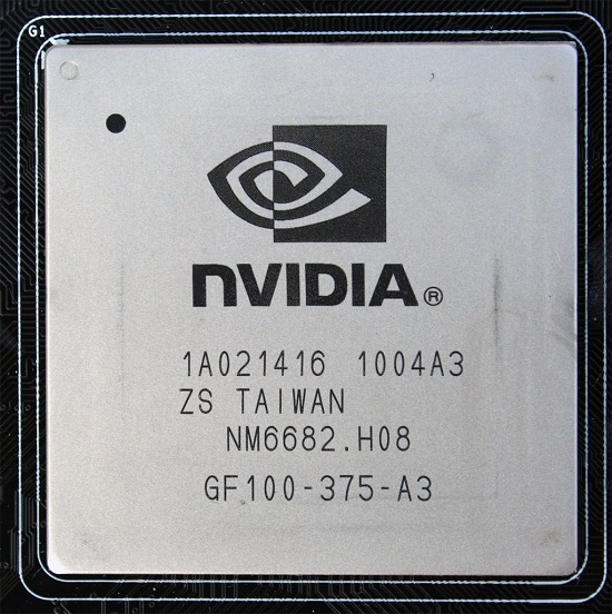
As most of you already know the architecture is code named Fermi, after italian physicist Enrico Fermi and physics is something that shines through the whole project – according to NVIDIA the delays have been because it couldn’t everything to work just they way it wanted. Here we are the result is the biggest update since the launch of the G80 architecture, launched in 2006, with the circuit named GF100 (GeForce Fermi 100).
There is little to no information on any other DirectX11 circuits from NVIDIA, but the company promises a transition to Direct X11 capable circuits across the lineup within 12 months. In lack of other relatives to analyze we can start dissecting GF100 right away. The architecture and a walkthrough of it can be found below.
GF100 core – 16 processors divided into 32 cores each
NVIDIA has chosen to the difficult path by building a huge die consisting of no less than 3.0 billion transistors. This in turn consists of 16 “Streaming Multiprocessors” (SM), I.e. something similar to CPUs that in turn have access to 32 CUDA Cores, shaders, these are similar to regular CP cores since these do the actual work. Each SM has 16/48KB L1 cache and on top of that a shared L2 cache at 768KB. The L1 cache is listed as 16 or 48KB because each SM has 64KB memory to access, but can split into 16KB L1 cache or used as shared memory, remaining 48KB will be used when needed the most.
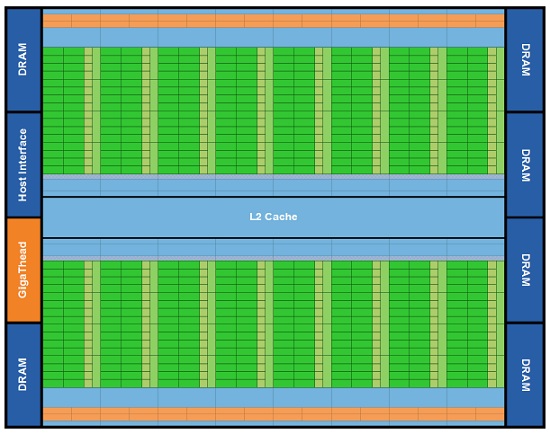
Structure of the GF100 core
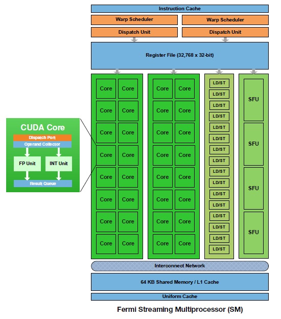
SM – Streaming Multiprocessor
After a short walkthrough of the core we feel that we have to compare NVIDIA’s two latest architecture, and as expected the new GF100 slaps the older G80 back into the stone age. This doesn’t necessarily mean dramatic performance improvements at all times, but it is clear that NVIDIA has designed GF100 for both programming support (with shared memory, L1 cache and L2 cache) and the previously mentioned physics bit that is best translated into FLOPS, in other words Floating Point capacity.
| GPU | G80 | GT200 | GF100 |
| Transistors | 681M | 1.4B | 3.0B |
| CUDA Cores (Shaders) | 128 | 240 | 512 (480) |
| Double Precision Floating Point Capability | – | 30 FMA ops/clock | 256 FMA ops/clock |
| Single Precision Floating Point Capability | 128 MAD ops/clock | 240 MAD ops/clock | 512 MAD ops/clock |
| Special Function Units/SM | 2 | 2 | 4 |
| Warp Schedulers/SM | 1 | 1 | 2 |
| Shared Memory/SM | 16KB | 16KB | 16/48KB |
| L1 Cache/SM | – | – | 16/48KB |
| L2 Cache | – | – | 768KB |
| ECC Memory Support | No | No | Yes |
| Concurrent Kernels | No | No | Up to 16 |
| Load/Store address width | 32-bit | 32-bit | 64-bit |
One thing you may have noticed with the table above is that GF100 is specified to have 512 CUDA Cores, while the GTX 480 launched today only has 480 cores. most likely this is because of the extremely complex manufacturing process that includes 3 billion transistors. We presume it had to give in and disable one unit to get a decent amount of working dies from each wafer, instead of repeating the catastrophe from the launch of GeForce GTX 280 where the availability was extremely scarce due to the complex and difficult to manufacture architecture.
For handling memory Fermi is designed a lot like an ordinary CPU. It has shared memory, L1 and L2 cache and 384-bits memory bus that is attached to GDDR5 memory (first time ever for NVIDIA) and for the first time it supports ECC memory.
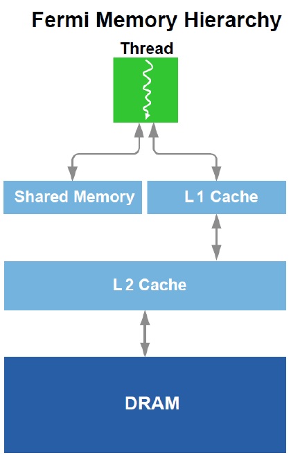
The memory hierarchy
On top of that NVIDIA has been working hard on its GigaThread technology, which is a way for executing multiple simultaneous threads, like modern CPUs, to use the full potential of the GPU, instead of queuing up commands. A very intuitive illustration can be found below.
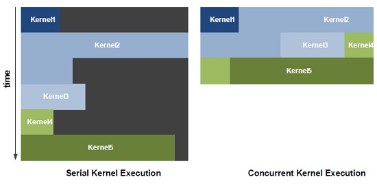
GigaThread i GF100 – executes your threads without pause
After this walkthrough of GF100 and its architecture we will reacquaint ourselves with DirectX 11 and its features and check what it has to offer against the competition.


