GeForce GTX 400 series - Specifications and competition
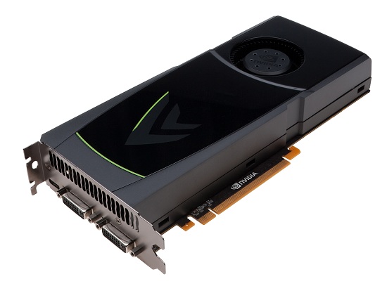
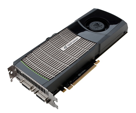
Moving on from all of the theoretic, let’s look at the actual cards launched today, GeForce GTX 470 and 480. Some pictures below.

NVIDIA GeForce GTX 470 – baby brother

NVIDIA GeForce GTX 480 – the flagship
The cards may not look that spectacular, both have two DVI ports and one mini-HDMI port. GTX 470 have a front made from plastic, while GTX 480 has a nickel coated aluminum cover on the front for maximal heat transfer. Exactly how GTX 480 is built up you will see further down the page, since we unlike GTX 470 has one of these to test. Let’s dig into some numbers first.
| GTX 480 | GTX 470 | GTX 285 | HD 5870 | HD 5850 | |
|---|---|---|---|---|---|
| Manufacturing node | 40nm | 40nm | 55nm | 40nm | 40nm |
| Core size | 529 mm2* | 529 mm2* | 470 mm2 | 334 mm2 | 334 mm2 |
| Transistors | 3 000 mil. | 3 000 mil. | 1 400 mil. | 2 150 mil. | 2 150 mil. |
| Shaders | 480 st. | 448 st. | 240 st. | 1600 st. | 1440 st. |
| GPU frequency | 700MHz | 607MHz | 648MHz | 850MHz | 725MHz |
| Floating point performance | 1.34TFLOPs | 1.08TFLOPs | 1,01 FLOPs |
2,7 TFLOPs |
2,09 TFLOPs |
| Texture units | 60 st. | 56 st. | 80 st. | 80 st. | 72 st. |
| Texture fill rate | 42.0 Gtexel/s | 34.0 Gtexel/s | 51.8 Gtexel/s |
68,0 Gtexel/s |
52,2 Gtexel/s |
| ROPs | 48 st. | 40 st. | 28 st. | 32 st. | 32 st. |
| Pixel fill rate | 33.6Gpixel/s | 24.3Gpixel/s | 20,7 Gpixel/s |
27,2 Gpixel/s |
23,2 Gpixel/s |
| Z/Stencil | – |
– |
–
|
108.8 GSamples/s |
92.8 GSamples/s |
| Memory type | GDDR5 | GDDR5 | GDDR3 | GDDR5 | GDDR5 |
| Memory frequency | 924 MHz (3696MHz) |
837 MHz (3348MHz) |
1242 MHz (2484MHz) |
1200 MHz (4800MHz) |
1000 MHz (4000MHz) |
| Bus width | 384-bit | 320-bit | 512-bit | 256-bit | 256-bit |
| Bandwidth | 177,4 GB/s | 133,9 GB/s | 159,0 GB/s | 153,6 GB/s | 128,0 GB/s |
| DirectX | DX11 | DX11 | DX10 | DX11 | DX11 |
| Max. consumption | 250W | 215W | 183W | 188W | 170W |
| Min. consumption | – | – |
–
|
27W | 27W |
| Price | $499 | $349 | $320 | $370 | $260 |
* NVIDIA doesn’t mention die size, it’s an estimate
The GF100 core is made with 40 nm technology, nothing odd about that. What is worth mentioning is that the number of CUDA Cores (shaders) is 480 for GTX 480, not 512 that was originally intended. Most likely this is the result of manufacturing problems and two SMs or 32 CUDA Cores had to be sacrificed. baby brother GTX 470 has to settle for 448 shaders and the already low frequency from GTX 480 lowered further, to the somewhat unorthodox 607MHz. GTX 480 spins at even 700MHz. The memory frequency is also a bit odd, 924 and 837MHz respectively, relatively low for GDDR5 memory since AMD’s high-end alternative HD 5870 spins at 1200MHz, SDR. This isn’t holding NVIDIA back to any significant degree though, since it has a much wider memory bus, 384-bit for GTX 480 and 320-bit for GTX 470, which results in 177.4GBps bandwidth for GTX 480.
Even though the card has relatively low clock frequencies three billion transistors adds up to a lot of power being consumed, something we will investigate closer. NVIDIA doesn’t mention “idle board power”, power consumed when the card is idle, where AMD impressed us with the HD 5000 series. Either way, GTX 480 is 62W above HD 5870, which gives some serious Radeon HD 2900XT flashbacks.
The next page discusses the sample of the day, GeForce GTX 480.


