


AMD Radeon HD 5870 - RV870 GPU and PCB
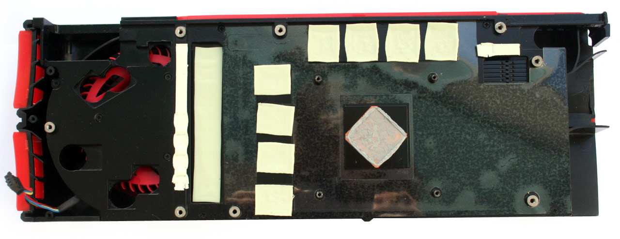
To access the actual card we have to remove 11 screws from the back of the card. This enables us to remove the back plate and then quickly realize there is nothing of interest there.
If you then remove the four screws that keep the actual GPU cooler in place you can remove the entire cooler from the card. This revealed how AMD has made sure that all of the hot components comes in contact with the beefy cooler and keep them at the right temperature.
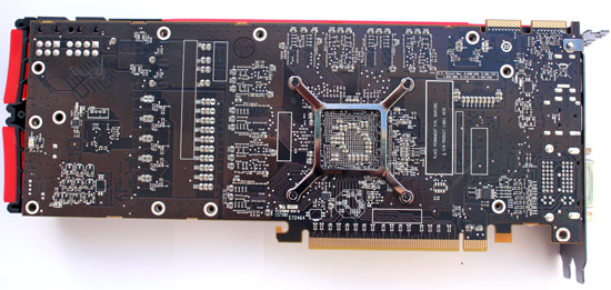
AMD has taken advantage of all 270 millimeters of the PCB and the RV870 GPU found in the middle is seated at an odd angle, a bit like previous generations. The graphics circuit is the only component with paste where other components use heat conducting tape instead, just to make sure there are not gaps.
The text on the GPU reveal little on the the properties of the chip for the uninitiated, but it’s pretty exciting that over 2 billion transistors hide beneath relatively small IHS.
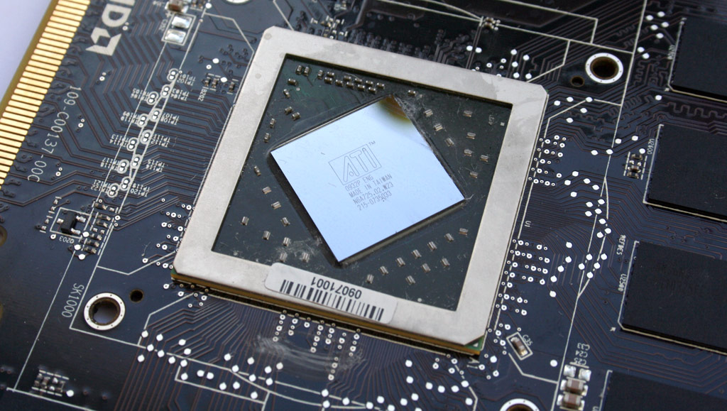 RV870 in all of its glory |
The GPU aside, there are eight 128MB GDDR5 memory circuits branded Samsung. The first Radeon HD 5870 cards will ship with a total memory buffer at 1GB while 2GB models will start shipping later this year.
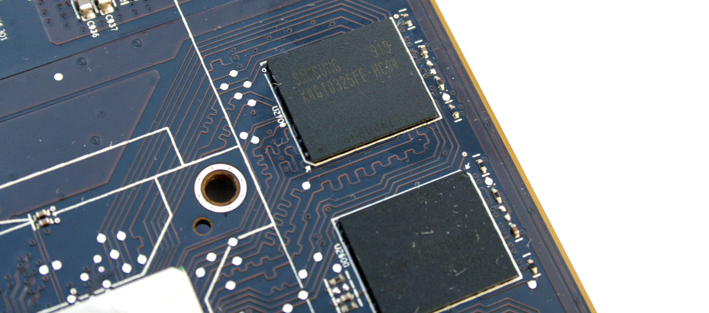 GDDR5 memory circuits from Samsung |
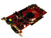
We round off with a short photo session starring AMD’s new graphics card flagship before we move on to the test system and benchmarks.
 |
 |
 |
 |
The voltage circuit from Volterra allows users to change the voltage through software, which makes overclocking a lot easier.


