


TSMC is the leading actor on the foundry market, and has just started mass production of 28nm circuits, but the largest retail products based on 28nm will not appear until later this year, or early 2012. The machinery is not standing still and it is discussing future plans and manufacturing processes.
While we are slowly reaching the physical limitations of how tight we can pack our transistors in a circuit, TSMC are not ready to stop but has detailed plans for its 14nm technology. The new technology will be the first to use some sort of 3D transistor to lower the increasing current leakage and it will also introduce 450mm wafers.
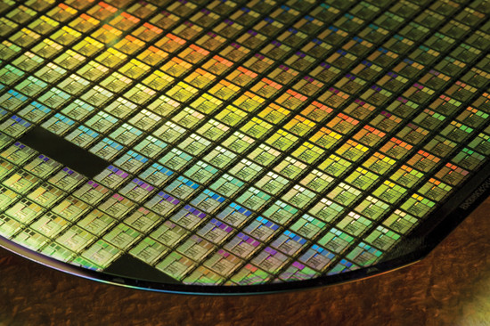
The advantage of 450mm wafers is that they can fit 125% more circuits than a 300mm wafer, this should lead to lower prices for TSMC clients – but also for TSMC. According to the head of development Shang-yi Chiang it will not need as many, or as large, plants as before after moving to 450mm wafers, which will lower captical costs for the new process. We can imagine that the tools needed for 450mm wafers will be very expensive initially, but be worth the investment in the long run.
Chiang says it will start development of 14nm in 2012, and is expected to start production in 2015. He adds that what is stopping TSMC from starting the development is not technological, but lack of engineers. The 14nm node will follow 20nm that both GlobalFoundries and TSMC is expected to start production with in 2013.
Source: guru3D


