Intel has been sitting calmly on the chipset-throne for a long time with their stable, fast and very overclockable circuits. Third party manufacturers like SiS, VIA and nowadays also ATi have had a really hard time making chipsets for Intel CPUs profitable. As if it isn’t enough that Intel already controls almost the entire market, the silicon giant from Santa Clara leaves nothing but crumbles for the competition. Among others, licenses has to be negotiated back and forth which Taiwanese VIA has experienced a several times.
Intel has been
sitting calmly on the chipset-throne for a long time with their stable,
fast and very overclockable circuits. Third party manufacturers
like
SiS,
VIA and nowadays also ATi have had a really hard time making chipsets for
Intel CPUs profitable. As if it isn’t enough that Intel already
controls almost the entire market,
the silicon giant from Santa Clara leaves nothing but crumbles for the competition.
Among others, licenses has to be negotiated back and forth which Taiwanese
VIA has experienced a several times.
The company has never given up the hope of getting a hold of some
bigger crumbles though. Instead, the development team has worked day
and night to make the ultimate weapon, VIA PT880. Ok, that might
have
sounded
a bit exaggerated but the fact remains that VIA PT880 is the company’s latest
chipset
for Intel CPUs and that it in theory looks like a dangerous opponent
to the monopolistic silicon giant.
We know though that not everything that looks good in theory pans out just
as good in real life, that’s why we have nagged on all mayor mainboard manufacturers
to supply us with a test mainboard based on the PT880 chipset.
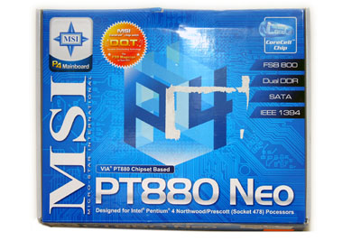
MSI was the first to reply and as a result it’s its VIA PT880 which will
be the first PT880 mainboard that NH reviews.
On the next page you will see a brief summarize of the PT880 chipset
before we take a closer look on the MSI-board.
VIA’s
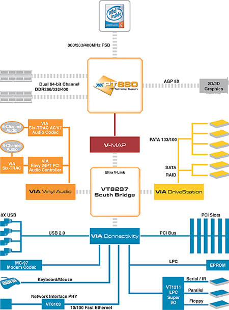
latest chipset for Intel CPUs is named PT880 and it offers a whole
lot of
interesting solutions. The chipset has support for all the P4 CPUs based
on the Northwood core, including the Extreme Edition versions. VIA also
claims
that the chipset is ready to handle the new Prescott CPUs. Of course
the chipset also support the Hyper-Threading technology.
The memory management is controlled by two 64-bits channels which in total
has support for up to 8GB internal memory of the types DDR266/333/400. To
optimize the memory management, VIA has introduced a technique they
call "Dual Stream 64" which is for reducing the memory latency and get a
faster memory prefetch. Furthermore, the new memory controller can also
run the memory asynchronous to the FSB. This means that it now is 100% possible
to use two DDR400 together with a FSB 533MHz-CPU without the memories
falling back to the DDR333 speed. Instead we get the maximum bandwidth of
6.4GB/s even without a 800MHz FSB CPU. The specifications also contain AGP
8x support, of course.
The link between the north- and Southbridge, which VIA has chosen to name
V-Link, has a theoretical maximum speed of 1066 MB/s. The Southbridge,
VT8237,
is an interesting little thing fully equipped with functionality. For
example it can handle, just as Intel’s chipset, up to eight USB 2.0 units
and, just as Intel’s ICH5R Southbridge, it has support for S-ATA RAID.
In the VIA
case it is not just a matter of RAID0 support but also support for RAID1.
The IDE channels are two to the number and have got support for up to
four ATA33/66/100/133 units.
The integrated sound is also an interesting story. The Southbridge supports
5.1-solutions through the AC97 codec but beyond that there is also the
option for the mainboard manufacturers to implement 7.1-audio. The
VT8237
circuit also offers network support for up to 10/100 Mbps Ethernet.
By clicking the links you can compare the VIA PT880 to
875 chipset and Intel’s
865 chipset in detail.
To judge by the specifications VIA seems to have gotten themselves a real
winner with PT880. The chipset gives a robust and powerful impression and
is
full of interesting features. The big question is if it can perform as well
as Intel’s own small miracle chips. The performance tests will reveal if
Springdale and Canterwood owners really have got something to worry about,
but until then it’s time for the ordinary story of the mainboards. We begin
with the specifications.
| Mainboard chipset: |
Intel
PT880 + VT8237 |
| CPU support: |
Intel Pentium 4/Celeron Socket-478, 533/800 MHz FSB |
| Memory Support: |
4xDIMM
266/333/400MHz DDR (MAX 4GB) |
| Integrated graphics processor: |
–
|
| AGP: |
1x
AGP 8X |
| PCI: |
5 x 32-bit bus master PCI |
| IDE controller: |
4
units, ATA 133/100/66/33 |
| RAID controller: |
–
|
| SATA controller: |
2x
150MB/s Through the Southbridge |
| Network circuit: |
Realtek
8201BL PHY 10/100Mbps |
| Audio circuit: |
6-kanals
Realtek 655 AC97′ Codec, S/PDIF out on the back (not optical) |
| FireWire
(IEEE-1394): |
–
|
| USB
2.0: |
4
x on the rear panel, 2 x through a bracket max 8 ports, |
| Price: |
~
800 SEK (Exchange rates) |
| Price and availability |
MSI’s PT880
Neo-LSR has a very competitive price. For example; the web shop Komplett.se sells
the mainboard for below 800 SEK which makes it cheaper than most Springdale-boards.
The price is in other words hard to beat. Unfortunately, the availability
is a bit worse as for today. There are some boards out
on the Swedish market
but the availability is a bit limited. But since the board is very new
this is probably a subject to change very soon when the demand increases
and more units
runs through the distribution channels.
| Accessories and features |
MSI’s PT880
is delivered with a standard set of accessories. When it comes to cables
there is one flat cable, one floppy cable, one S-ATA-cable with a
power converter to match, and last, a two ports USB 2.0 bracket. The bracket
is a bit special since it is equipped with “Debugging LEDs”.
Four LEDs on the back is lit and put out in different combinations during
the boot process to show what stage of the boot process
the
system is, a convenient extra function that surely has helped
quite a few computer builders to find out what’s wrong.
The documentation consists out of one manual and a quick installation booklet
for those who don’t have the energy to look through the thicker manual.
A CD-Rom is also a part of the package which contains the necessary drivers
and some useful software; for example MSI’s own Windows based overclocking
tool Fuzzy Logic.
We have summarized
all accessories you can find in the carton below.
| Accessories: |
|---|
|
1
x 80-pins ATA cable, 1 x Floppy cable |
|
1
x Serial ATA150 cable and S-ATA power cable converter |
|
1
x mainboard manual, 1 x “Quick User’s Guide” |
|
1
x Installation CD-Rom with drivers and useful software (Acrobat Reader, PC-Cillin, PC Alert, Fuzzy Logic, Live Update) |
|
1
x two port USB 2.0 bracket with Debugging LEDs |
MSI’s PT880
Neo is a board with many features mostly because of the powerful Southbridge
VT8237 which offers excellent expansion possibilities. For example you
can connect up to 8 USB 2.0-units, but you have to use another two ports
bracket
in addition to the one that comes in the package. Furthermore the chipset
has Serial ATA support which comes in the form of two orange colored S-ATA-ports
located close to the right of the Southbridge. Integrated network circuit
is also available in the form of Realtek 8201BL PHY which delivers
10/100 Mbps Ethernet.
Realtek has also contributed with the sound circuit that along with the
Southbridge delivers
5.1-sound through the AC 97′ codec. Unfortunately Firewire support is missing
but there is a more expensive Firewire version of the board for those who
absolutely
must have Firewire.
Overall MSI’s PT880 Neo is a well balanced board especially considering the price.
We have reached
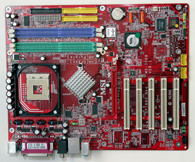
the section where we take a closer look at the mainboard’s layout. We begin
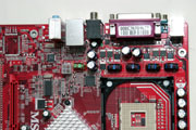
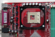
on the upper side of the board, the socket area in other words. There is
a lot of space around the socket apart from the upper row
of capacitors. Installing the cooler is a piece of cake and we are very
happy
that the
CPU-fan’s power connection is at the top against the mainboards’ edge
and not squeezed in between the socket and the DIMM-slots that so many
other boards have.
The 12V-contact is a bit worse located though, a bit down near the rear panel.
Certainly, it’s still very easy to access it since there are no disturbing
capacitors around it, but it’s hard to minimize the horde of cables when
you have to
pull the cable all across the case. The ATX contact is very well placed
on the right edge. To the left we find the four DIMM-slots and to the right
the floppy contact. Below we can see both of the yellow IDE-contacts.
 |
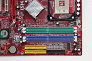
The distance
between the AGP-slot and the DIMM-slots is rather long making it very simple
to install the memories without having to remove the graphics card, even
if you have a very large graphics card.
This area in particular is usually very narrow to work in and that makes
it extra sweet to see that MSI really worked with the placement of the
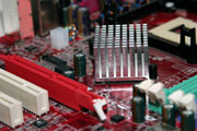
components. The Northbridge, PT880, is as we can see from the pictures
below cooled with
a passive heatsink. No whining Northbridge cooler to worry about. We’ll
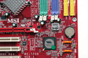
stay in the area below the DIMM-slots since it is the board’s most interesting,
since we find both the Southbridge and the CoreCell circuit here. The
CoreCell
circuit is MSI’s equivalent circuit to ABIT’s u-Guru. The two orange
contacts we see in the middle picture are the two S-ATA-channels that are
controlled
by the Southbridge. Unfortunately there is no RAID-support which is on
the other hand a bit much to demand from a chipset as cheap as the PT880.
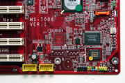
On the picture to the right we can see both internal USB-contacts that through
brackets make it possible to use up to four USB 2.0 units. The bracket that
is delivered with the mainboard is only equipped with two ports though, so
you have to get you hands on an extra bracket if you want to use all ports.
In the lower right corner we can see the connections to the case speaker,
reset button, power button etc.
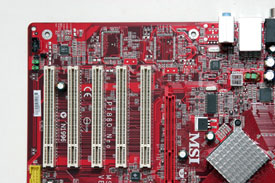
If the integrated
features aren’t enough for you, you can just add different expansion cards.
PT880 Neo is equipped with five PCI-slots that most people should have a hard
time
to
fill.
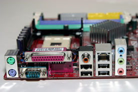
On the
rear panel we find the PS/2-contacts for mouse and keyboard, COM and
serial port, four USB 2.0-contacts, network connection, an S/PDIF-out
and the connections for the sound circuit.
The layout of the
MSI PT880 Neo is among the best I’ve seen in a very long time. The board feels
very "spacey" without any narrow regions. The only remarkable thing
is the 12V-contact that could have been placed on the top of the board instead.
Other than that MSI has really made good job concerning the layout.
We congratulate and move on to the BIOS-section that hopefully will be just as much pleasure.
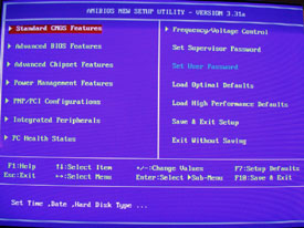
MSI
has been been faithful to American Megatrend’s AMIBIOS for a long time which is also what we find in the heart of the PT880 Neo mainboard. The mainmenu reminds me a lot of the one that Phoenix AwardBIOS uses but if you look closely to the headlines you quickly notice the differences.
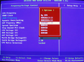
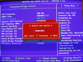
"Frequency
Voltage Control" contains the overclocking settings which we begin with as ordinary.
Here we find the settings for the processor’s FSB, the memory ratio and the necessary voltage settings. More precise values for these can be found below in the table at the end this section. The really interesting bit here is that you can run the memory out of synch with the processor speed. That is if you don’t use a FSB800 MHz CPU. In practical terms it means that you can have the memory running at Dual Channel DDR400 despite the fact that the CPU only runs at FSB133 (FSB533 efficient) something that isn’t possible on any Intel chipset without also overclocking the processor bus.
Further more there are possibilities to adjust the chipset voltage which is very unusual.
Last but not least we want to bring your attention to the "Dynamic Overclocking"-function.
This function will automatically overclock the system when the Core Cell-circuit notices that the workload increases, for example when starting up a game. When the workload decreases the system is downclocked again to avoid any extra wear. The amount of overclocking is determined by the six presets from which you can choose from in the menu. The Dynamic Overclocking-function is practical but alas it doesn’t really say what difference there is between the presets, or how much they really overclock. If you want to keep maximum control it’s best to configure your overclocking manually.
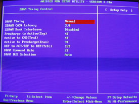
"Advanced
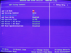
Chipset" is divided into a main menu with two submenus.
Under submenu number one we find the memory timings and ratio while under submenu number two we can adjust the AGP-settings.
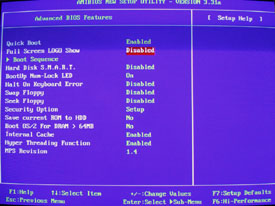
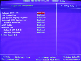
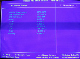
The cards integrated features are adjusted in "Integrated Peripherals". The PC-Health section shows as it says the system’s "health" in terms of temperature and voltage readings.
In the table below there is a summarize of the mainboard’s overclocking settings.
|
BIOS-settings
|
|
| FSB-frequency: |
FSB400:100-355MHz/FSB533: 133-388 MHz FSB800: 200-455 MHz |
| AGP-frequency: |
fixable,
anywhere between 66.9-100.9MHz |
| CPU-voltage: |
CPU-default-1.6v in 0.0125v steps |
| DIMM-voltage: |
2.5v
– 2.9v in 0.05v steps, 2.9v-3.3v in 0.1v steps |
| AGP-voltage: |
1.5v
– 1.9v (0.05v steps), 1.9v-2.2v (0.01v steps) |
| Northbridge: |
1.62v
– 1.80v (0.06v steps) |
| Southbridge: |
2.5v
– 3.0v (0.05v steps) |
The PT880 Neo mainboard is equipped with a very powerful BIOS that bodes well for the overclocking tests. The settings are very generous and there is really everything you might need for squeezing every single last drop out of your components. Well almost anyway. The processor voltage
maximum value of 1.60 V is a bit low especially for overclockers using water- or compressorcooling. A maximum value of 1.85v had been been better. We’ll have to hope for a BIOS-update that will change this. Except from this little mistake the mainboard’s BIOS is awesome.
| MSI
Core Center & Live Update 3 |
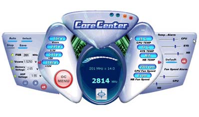
Core
Center is MSI’s equivalent to ABIT’s u-Guru. Certainly MSI was first its Core Center-concept but for some reason it feels like a good comparison. The Core Center-application’s task is to monitor temperatures, voltage readings,
fan speeds, clock frequencies plus, and this is the best part, to overclock the system while you are using
Windows.
On the picture below you can see the Core Center application with its functions folded out on the side. The middle part of the application shows the clock frequencies, temperatures and voltage readings while on the right "wing" we find settings for the threshold values where the system should warn or turn off the computer. On the left wing we find the overclockingsettings.
FSB, Vcore, DIMM-voltage and AGP-voltage can be adjusted by clicking the wanted value and then press the "+"
or "-"-button in the lower part of the menu. Further more there is an "AUTO"-function which will automatically overclock the system as long as it seems safe to do so. If you want to manually stop the clock during automatic overclocking you simply press the "Stop"-button.
The big red "OC Menu"-button folds out another menu which lets the user overclock the system with the memoryspeed as centerpoint. Here the user can choose between a number of presets for memory ratio such as DDR433/450/500
.etc. For example of you pick DDR450 the processor will be overclocked to 250MHz FSB which with 1:1 memory ratio will lead to an efficient memory frequency of DDR450 MHz.
The Core Center-software worked very well in our tests. The possibility to adjust both processor speed and voltages makes the application a very powerful and neatly packaged application which definitely should be used if you own MSI-mainboard with Core Center support.
Live Update 3 is not a part of the Core Center-package but an independent application which makes it possible to update the mainboards’ BIOS, graphics card-BIOS (if you own a MSI graphics card), mainboard-drivers, graphics card-drivers and the useful software Live Utility and Live Monitor via Internet.
Through a few clicks you can download and install above mentioned updates in Windows without any inconvenient Start-up diskettes and similar.
| Overclocking |
230 MHz FSB,
the highest clockfrequency our test processor can manage with aircooling,
turned out to be no problem for MSI’s
VIA PT880 Neo. A small increase of processor voltage was everything that was required to keep perfect stability in overclocked mode. VIA’s PT880 chipset seems to be able to compete with Intel’s own chipset not only on both
the price- and feature-front but also when it comes to overclocking,
something that thirdparty manufacturers usually has a hard time with.
The testsytem’s
configuration is next.
|
Test
system |
|
|
Hardware
|
|
| CPU: |
Pentium 4 2.8GHz (800 MHz FSB)
|
| Mainboard: |
Reviewed sample: MSI PT880 Neo-LSR Reference boards: AOpen EY65 XCube (i865G) Shuttle ST61G4 (Radeon 9100 IGP) Shuttle SB75G2 (i875P) |
|
RAM:
|
2
x 256MB GeIL PC3500 Ultra CL2, 2 x 512 Corsair DDR500 |
|
Graphics
card: |
nVidia GeForce FX 5900 Ultra 256MB @ 450/850MHz
|
|
Harddisc:
|
80GB Maxtor 740DX
|
|
Software
|
|
| Operative
system: |
Windows XP Professional SP1
|
| Resolution: |
1024x768x32bit, 90Hz
|
| Drivers: |
Detonator
53.03 WHQL DirectX 9.0b Intel chipset driver 5.1.1.1002 VIA Hyperion 4-in-1 v1451 |
|
Benchmarking software:
|
3Dmark2001
SE 330 Audioactive Production Studio 2.04j (Fraunhofer II encoder) Comanche 4 benchmark Mpg Mediator DivX 5.1.1 encoding PcMark 04 Quake 3:Arena v1.32 SiSoft Sandra 2004 Terragen Oshyan Bench Unreal Tournament 2003 demo v.2206 WinRar v3.20 WCPUID |
With all boards we used the following timings: 2-6-3-3
AGP Aperture was set to 128MB.
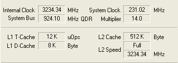
Before we begin with the benchmarking we check the mainboard’s real frequency at 200 MHz FSB with WCPUID.
|
|||||||||||||||||||||||||||||||||||||||||||||||
The MSI
board is 1 MHz above FSB 200 MHz. However the worst one is AOpen EY65 though, which has a frequency of 201.64 MHz
It’s time to find out what the VIA PT880 chipset has to offer.
|
||||||||||||||||||||||||||||||||||||||||||||||||||||||||||||||||||||||||||||||||||||||||||||||
|
||||||||||||||||||||||||||||||||||||||||||||||||||||||||||||||||||||||||||||||||||||||||||||||
Already
from the start MSI’s PT880 makes a good performance. The optimization
of the memory they have made on the chipset has really paid off
since the PT880 mainboard in performance lands right between the
Springdale- and Canterwood-reference boards.


