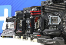
Gigabyte GA-965P-DS3 is on paper a very promising board and in our latest article we overclock the board to find out how much extra value you can collect.
Ever since Intel’s introduction of the Core 2 series of CPUs it has reclaimed its position on the great throne of processing performance from AMD, and at the same time it doesn’t even have to cost that much. No one who is up to date can have missed the Core 2 series and its performances around the world in the hands of enthusiasts and even though the choice of CPU might be crystal clear for many, you have to think harder about which motherboard you might want to pick.
Today, we are looking at four “more” high end chipsets supporting Allendale/Conroe/Kentsfield; these are Intel’s own 965P and 975X, ATI’s RD600 and NVIDIA’s 680i. The three latter comes with a big drawback though; they far from cheap.

Think of it like this. You’re in a situation where you’re aiming at an Intel Core 2 Duo E6300 or E4300 CPU and you have a budget of about $150 to spend on a motherboard. Of course you’re looking to get the best one available for this kind of money. You look around at several retailers, just to realize that there are more or less only boards with the 965P chipset available. Then it all takes a turn for the worse; which one of all these should you choose? We hope to find out if Gigabyte’s competitor, the GA-965P-DS3 is up to the challenge, and we’re not determining whether it’s good or not by measuring USB and Ethernet performances. It’s all from the enthusiast’s point of view.
Gigabyte GA-965P-DS3 |
|
| Processor support | Intel Core 2 Extreme Quad-Core / Core 2 Duo / Intel Pentium Extreme/ Intel® Pentium D processor |
| Chipset | Intel P965/ICH8 |
| Memory | 4x 240-pin DIMM Unbuffered ECC/Non-ECC Dual Channel DDR2 800/667/533 Max. 4GB |
| Expansion slots |
1x PCI-Express x16 |
| Storage |
1x Floppy |
| Internal connections |
6x USB |
| External connections |
1x PS/2 Mouse |
| Size | 305 x 215mm |
| Price | ~$125 |
You simply can’t judge by the specifications, since nothing really stands out. There’s one point of confusion though, and that’s the apparent lack of support for Celeron, but hopefully no one will miss this. Also, support for future 1333FSB CPUs are supported since BIOS revision F9.
Enough with the specs already, let’s have a look at the card itself. Off to the next page!
The first thing you encounter when you look at the GA-965P-DS3 is the mix of colors, certainly not for the faint-hearted, as we’ve experienced among the crew here at NH. You can’t pin the color coding down though, contrasts among the connectors isn’t what we’re missing. It’s a bit of a fruit-salad, but whether it’s good or bad is up to you to decide.
But let’s have a look at the board itself then, to begin with:
 |
As earlier mentioned, the first thing that hits the eye is the mix of colors. If you decide to look past all the colors you actually notice it’s a very nice layout with no strange placements of connectors whatsoever, except maybe the IDE connector which didn’t quite fit next to the FDD and ATX connectors. This is the only flaw that comes in mind with the layout, although this probably won’t be much of a problem for anyone. Also, the board is not as wide as standard ATX sized motherboards, it’s three centimeters short, stopping at 21.5cms compared to the ATX standard 24.5cm. This makes the impressive layout even more impressive.
 |
 |

|
If we take a look around the socket we discover small potential problems with capacitors and voltage regulators between the mounting holes for the cooler. This wasn’t any problem during our testing, with neither Intel’s stock HSF nor the Noctua NH-U12. The CPU is fed its currents via a three phase regulation system which does its work flawlessly, even delivering voltages up to 2.0V, more of this later.
 |
Further on, we have a northbridge heatsink with a quite hard task ahead, namely keeping the 965P chipset cool. But since someone has placed it there, it should be able to do its work without complications.
Below, we’ve gathered more or less random shots of the card, if you wish to see them in a higher resolution, just click and enjoy.

|
 |

|
 |
|
|
We have to end it somewhere, hopefully the images were to your satisfaction. Let’s move on to a look at the BIOS.
Our sample was shipped with the F6 BIOS which offered enough overclocking options, but we figured the latest BIOS revision F9 would be better for overclocking. The F9 also supports 1333FSB CPUs when they finally arrive. Said and done, the F6 got replaced more or less instantly. But what does the BIOS look like?
 |
As you can see, a very ordinary Award layout, nothing to rant at. This is without the somewhat frustrating Ctrl+F1 function though.
 |
This is what BIOS looks like when you’ve pressed Ctrl+F1. Nothing new at a first glance, but if you look closer you see a new menu, Advanced Chipset Features.
Happily, we check it out:
 |
It wasn’t that exciting, to say the least. Not as advanced options as the name led us to believe, especially when it required the Ctrl+F1 function to show up.
 |
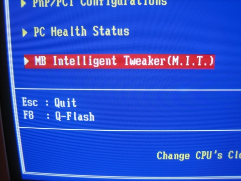
But this is where the fun starts. The overclocking menu, or M.I.T., MB Intelligent Tweaker as Gigabyte has chosen to call it. What fun things does this menu bring to the table?
.jpg) |
 |
To the left, you see M.I.T. without the Ctrl+F1 feature, to the right you see what it’s like with Ctrl+F1. A very nice bunch of timings has showed up, which of course is nice.
 |
 |
The Gigabyte engineers also seem quite confident of what they’re doing when it comes to the currents. If you decide to change the "System Voltage Control" from "Auto" to "Manual" you get to stare at a blinking red text which probably is supposed to scare you away if you’re a beginner or just unsure.
 |
 |
Gigabyte has been kind enough to let their users feed 2.5V to the RAM, this could well come in handy whilst overclocking. This is a point where the F9 BIOS differs itself from the F6, the F6 only had 2.4V, +0.6V maximum. Also the PCI-E voltage ought to be enough. This is a voltage that doesn’t require tampering often, and it probably would be able to start causing serious damage if you set it higher than +0.1V.
 |
 |
VFSB, or FSB OverVoltage Control is also adequate with its +0.3V. +0.3 is also max on the 965P chipset, called (G)MCH in BIOS, is also good to see. Just make sure you’ve got enough airflow around the chipset cooler, as the northbridge tends to get quite hot.
But what’s the most interesting thing in practice? That’s right, VCore. The options are seen below.
 |
 |
You just have to be impressed by voltages all the way up to 2.0V. The increments above 1.6V are way too harsh though, 0.2V increments are way too big if you’re not having a barbeque. Anyways, all the way up to 1.6V you have very fine increments of 0.00625V all the way from 0.5125V, which could come in handy if you would like to run your Prescott with bearable heat dissipation.
Since you made it all the way here, you probably want some tests, right? And you got it, go to the next page.
|
|
| Hardware | Test system |
| Motherboard | Gigabyte GA-965P-DS3 |
| Processor | Intel Core 2 Duo E6300 (627/629) |
| Memory | Geil GX22GB6400UDC |
| Graphics card | X1950XT 256MB |
| Power supply | OCZ Powerstream 520W |
| Software | |
| Operating system | Windows XP (SP1a) |
| Chipset drivers | Intel 8.1.1.1010 |
| Graphics drivers | Catalyst 6.12 |
| Benchmarks | SuperPi 1.5 WinRar 3.61 Cinebench 9.5 |
So, here we are, the page you all have been waiting for. That’s right, overclocking of the motherboard. The board itself is really nice to overclock, there’s no problems at all to get over 480FSB, but then something happens. Around 485FSB things don’t act quite as stable anymore, but around 80% of the time you’re able to boot the computer and run a few performance tests. Whilst overclocking in Windows you can hit 492 and take a screenshot in CPU-Z if you’re quick enough, but after that it freezes pretty much instantly.
This could be the CPU itself though, as the Core architecture actually sets the limits on some CPUs.
Anyway, 480FSB is fully stable and that’s the frequency we’ve chosen to run our tests at, and for comparison we’ve chosen to look at how things perform at standard frequencies from both the bus and frequency perspective. (266×7, 310×6, 480×6 480×7)
Let’s take a look at some results in Cinebench, an application that mainly tests the CPU, but doesn’t really care about the bandwidth.
 |
 |
We’re looking at a very strange thing here, the motherboard performs worse in 310×6 compared to 266×7 even though the RAM is running 1:1 and the timings are identical. The 6.6MHz difference shouldn’t cause any measurable difference either, until further notice we’ll just have to wait and see what results further tests bring.
Let’s check out how the CPU and motherboard perform at 480×6 and 480×7:
 |
 |
No real surprises with 895 and 1029CB-CPU. The scores are scaling as they should, no more, no less.
But what kind of results do we get in SuperPi 1M?
 |
 |
To say the least, it’s a very confusing result, SuperPi if anything benefits of higher bandwidth. At the same clock frequency on CPU but higher on the RAM, the result should be more like a half a second better rather than worse. But on the other side, we have no intentions of stopping here; let’s check on 480×6 and 480×7.
 |
 |
This is where the real fun begins. Less than 20 seconds with 480×6 with timings set by the motherboard all by itself, which rendered in not all too great 5-8-8-20. 17.375s at 480×7 with the exact same timings, nothing to complain about. Worth to note is that there is probably a half of a second to shave off if you wish to start tweaking the timings, but that’s nothing we’ll do in this article.
But let us take a look at yet another application that benefits from high bandwidth. Say hello to WinRar.
 |
 |
We see it again, 310×6 is in practice worse than 266×7 despite higher memory bandwidth. A very interesting phenomenon to say the least although we probably could blame this on Intel’s 965P chipset, which isn’t exactly consequent in all situations. But what’s most important is that the mainboard has been performing perfectly in 480×6 and 480×7 in the test so far, and that makes up for the issues with ease.
 |
 |
WinRar shows us that it doesn’t care that much about raw clock frequency on CPU but that it likes high bandwidth, something you at least are supposed to have loads of running DDR2 in 960MHz.
We are not saying you don’t get performance boosts in other applications though, as we’ve clearly seen that in Cinebench and SuperPi. The only thing that left us confused is the differences between 266×7 (stock frequency) and 310×6, as 310×6 should be at least a tiny bit better performing, but machinery isn’t always performing as it should. We just have to overlook this little problem, as it really could be pretty much anything, although we reckon the cause of the problem would be the chipset. Why we overlook it is because this article wasn’t written with running 310×6 in mind, especially not when you have more than 50% of the system bus left to overclock and higher multipliers to use, on our sample.
After a few weeks with the Gigabyte GA-965P-DS3 I’m stuck. It’s not specially hard to see why if you’ve ever owned a Gigabyte motherboard. At least personally, yours truly has never had any problems with earlier Gigabyte products, and luckily this is no exception.
Just look at the pricing. It’s not among the more expensive motherboards today, but it doesn’t leave you longing for more. The system bus could have been more overclockable but bearing the possibilities of CPU limiting the overclock we can’t blame the motherboard for it fully. Furthermore, the board has a small handicap in form of the C1 stepping of the P965 chipset, although these are being phased out for chipsets with C2 steppings.
Whilst we’re at it, let us tell you that the GA-965P-DS3 rev 2.0 is already out in stores being sold under the original name. These are equipped with the C2-stepped chipsets, which allow higher overclocking. An additional new revision, 3.3 is also on its way with native support for 1333MHz FSB.
But to stay in the present, we still have an evaluation to do, in addition to the overclocking potential.
BIOS
Gigabyte has generally had very user-friendly BIOS, although these might not be the most straightforward BIOS incarnations that has ever been made, they are still very good. Things have found the right places under the menus, you don’t need to take a day off to change something in your BIOS. Everything is logically placed, just as it should. The only thing that really bothers is the Ctrl+F1 function, it feels quite silly to be able to be able to set 2.0V VCore without it, but not to be able to shut down the integrated NIC. On the other hand, there’s a good bunch of memory timings to play with, something we always welcome.
Voltages
The ability to set currents is really generous, even though you might want to wonder about 2.0V to the CPU without even the Ctrl+F1 function in BIOS. The increments between 1.6V and 2.0V are quite harsh as well with 0.2V steps. The very exact 0.00625V steps could have existed here as well, even though you don’t use voltages in excess of 1.6V every day.
2.5V VDimm is also good to have, at this voltage you better have at least a fan blowing towards your RAM, although this wasn’t the subject of our evaluation. The increments between 1.8V and 2.5V is 0.1V which could be a bit harsh as well, although you don’t benefit of finer increments that often.
The VFSB is can be set to a full +0.3V with 0.1V increments which we welcome, as this could come in handy at higher frequencies.
+0.3V comes again when we look at the voltage settings for the Chipset, although you better have a nice airflow around the heatsink as it gets very hot. The 0.1V increments are present here as well.
The last one we take a look at is the PCI-E voltage, which we’re able to set to +0.1V or standard. This shouldn’t do any major difference but all too high voltages here could potentially da mange your graphics if you’re unlucky.
Stability
This is the point where the Gigabyte engineer’s has been working hard, you feel it. Either the card works fully day in and day out, or not at all. The few times you don’t get it working is when you’ve set something wrong in BIOS and the motherboard actually resets itself more often than not, so you don’t have to start unscrewing side panels on cases if you happen to have one of those, in order to reach the CCMOS pins. All in all, this is a motherboard that pretty much takes on everything thrown its way and doesn’t let you down.
Overclocking
Overclocking was the main subject of this article, unluckily we encountered a few problems in our path. During the time we’ve evaluated the overclocking possibilities we haven’t had access to more than two E6300 CPUs, whereof one was a really bad one. 480FSB fully stable would probably be the CPU’s or the C1 stepping on the chipset’s “fault”. There is a whole lot more to be uncovered, the world record with a GA-965P-DS3 with a C1 stepped northbridge is over 600FSB, although this was with liquid nitrogen on the chipset. Many enthusiasts has ran far beyond 500FSB with their DS3’s, so 480FSB is not the absolute max, it’s far from the truth.
Conclusion
Gigabyte is a brand stands in the shadows of many other manufacturers, which we think is a shame. More competition benefits the consumers of course, but Gigabyte’s current lineup of Conroe motherboards deserves more attention. You most certainly won’t be in need of higher voltages, the boards already have C2 northbridges with a bit of luck and nothing is downright bad with this motherboard. We hope to see Gigabyte motherboards in the hands of more enthusiasts, yours truly sends his regards from the light side.
Unfortunately our judgments are clouded somewhat by the C1 northbridge our motherboards sports. If the C2 models handles just as well we would’ve given it an award, but right now GA-965P-DS3 isn’t quite there.
|
|
|
Gigabyte |
|
Pros Cons |
We would like to thank Gigabyte for supplying the sample.


