NVIDIA wasn’t at all interested in supplying any information on the physical measurements of GF104 at the launch of GeForce GTX 460. The reason is probably the less flattering size that from a pure manufacturing perspective puts NVIDIA in a tight spot.
When NVIDIA developed the second version of Fermi it decided to cut the GF100 GPU in half, and refurnish some of the interior. The result was a relatively powerful GPU with low power consumption and no more heat problems.
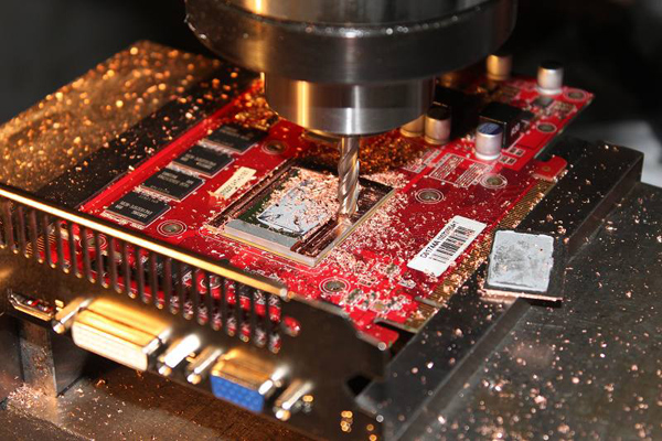
To users and consumers this is really everything you need to know, but for NVIDIA it’s a bit more complicated. The first pictures of the physical GeForce GTX 460 core has been published online, pictures taken after removing the heatspreader from the graphics circuit, the hard way.
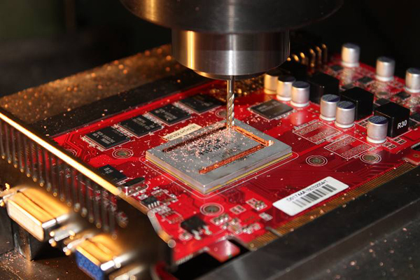
The pictures reveal a rectangular graphics circuit that even if it is smaller than big brother GF100 is still bigger than the AMD Cypress GPU, the GPU used by head foe Radeon HD 5830, but also the much faster and more expensive Radeon HD 5870.
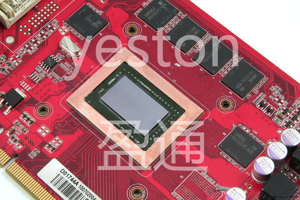
Early information has claimed a surface area of 366mm^2 with GF104, which is confirmed by these pictures. You can compare this to the 334mm^2 of Cypress and simply it means that NVIDIA can’t make as many GPUs per silicon wafer as AMD can, and that the GF104 GPU is still more expensive than AMD’s most expensive Cypress chip. This is no matter the quality of the manufacturing ot day, where AMD probably has the advantage with its more mature technology.
Keep in mind though that GF104 is sold at around $240 with GeForce GTX 460 1GB, while AMD is selling Radeon HD 5870 for around $360, even though the chip is considerably cheaper to manufacture.
The positive note for NVIDIA is that GeForce GTX 460 is a great graphics card with a well balanced GPu. The negative is that the cost margins are nowhere near those of the closest competitor.