


Annons:


Nyheter

M4 iPad Pro är Apples tunnaste produkt hittills
Under sitt senaste event avtäckte Apple fyra nya iPad-surfplattor och den nya systemkretsen M4....

Ny information om Nintendo Switch 2 bekräftad
Trots att Nintendo Switch 2 inte har avtäckts ännu var en tillbehörstillverkare lite för...

AMD ger RDNA 4 helt ny design på raytracing-hårdvaran
AMD sägs nu bygga upp hårdvaran för raytracing i kommande arkitekturen RDNA 4 från...

Windows 11 har nu officiellt reklam i startmenyn
Vi har sedan tidigare vetat att Microsoft planerat att trycka in reklam i startmenyn...


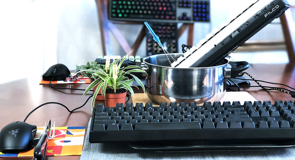
Svenska Tangentbordsguiden
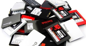
Svenska SSD-guiden
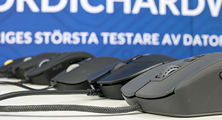
Svenska Musguiden

7 Days to Die lämnar early access efter 12 långa år
Speltiteln 7 Days to Die har varit ute i early access-utförande i hela tolv...

Krönika: Är Intel/AMD/NVIDIA de sista överklockarna?
Kända överklockaren Tobias "Rauf" Bergström tar ton och menar att hårdvarutillverkare pressar sina komponenter...

Ghost of Tsushima får officiella systemkrav för PC
Sony fortsätter arbetet med att ta tidigare konsolexklusiva speltitlar till PC och härnäst är...

Playstation 5 Pro kan ha fått sina specifikationer röjda
Ryktena kring Playstation 5 Pro fortsätter hagla och nu sägs utvecklingsenheter ha landat hos...