


Annons:


Nyheter

AMD ger RDNA 4 helt ny design på raytracing-hårdvaran
AMD sägs nu bygga upp hårdvaran för raytracing i kommande arkitekturen RDNA 4 från...

Windows 11 har nu officiellt reklam i startmenyn
Vi har sedan tidigare vetat att Microsoft planerat att trycka in reklam i startmenyn...

7 Days to Die lämnar early access efter 12 långa år
Speltiteln 7 Days to Die har varit ute i early access-utförande i hela tolv...

Krönika: Är Intel/AMD/NVIDIA de sista överklockarna?
Kända överklockaren Tobias "Rauf" Bergström tar ton och menar att hårdvarutillverkare pressar sina komponenter...


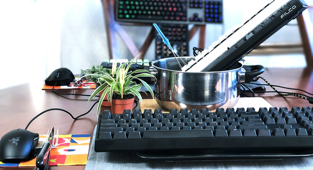
Svenska Tangentbordsguiden
Svenska SSD-guiden

Svenska Musguiden


Ghost of Tsushima får officiella systemkrav för PC
Sony fortsätter arbetet med att ta tidigare konsolexklusiva speltitlar till PC och härnäst är...

Playstation 5 Pro kan ha fått sina specifikationer röjda
Ryktena kring Playstation 5 Pro fortsätter hagla och nu sägs utvecklingsenheter ha landat hos...

Moddare ger World of Warcraft VR-stöd
Den som önskar bo i Azeroth har på ett ungefär fått sina böner hörda...

Remnant 2: The Forgotten Kingdom lanseras 23 april
Gunfire Games fortsätter arbetat på Remnant 2 och har nu avtäckt Remnant 2: The...