


Annons:


Nyheter

Ubisoft stänger ner The Division Heartland efter flera års utveckling
Ubisoft avtäckte under 2021 spelet vid namn The Division Heartland. Detta skulle bli en...

Epic Games får miljonbot – ska ha misslett minderåriga i Fortnite
Epic Games har förlorat i en Nederländsk rättegång där man anklagats för mörka mönster,...

AMD sjösätter grafiklösa Ryzen 7 8700F och Ryzen 5 8400F
AMD rullar nu ut två processorer kallade Ryzen 7 8700F och Ryzen 5 8400F....

RDNA 5 blir helt ny arkitektur – RDNA 4 blir mest buggfixar
AMD:s framtida grafikarkitektur RDNA 5 sägs bli en slags nystart och byggs helt från...


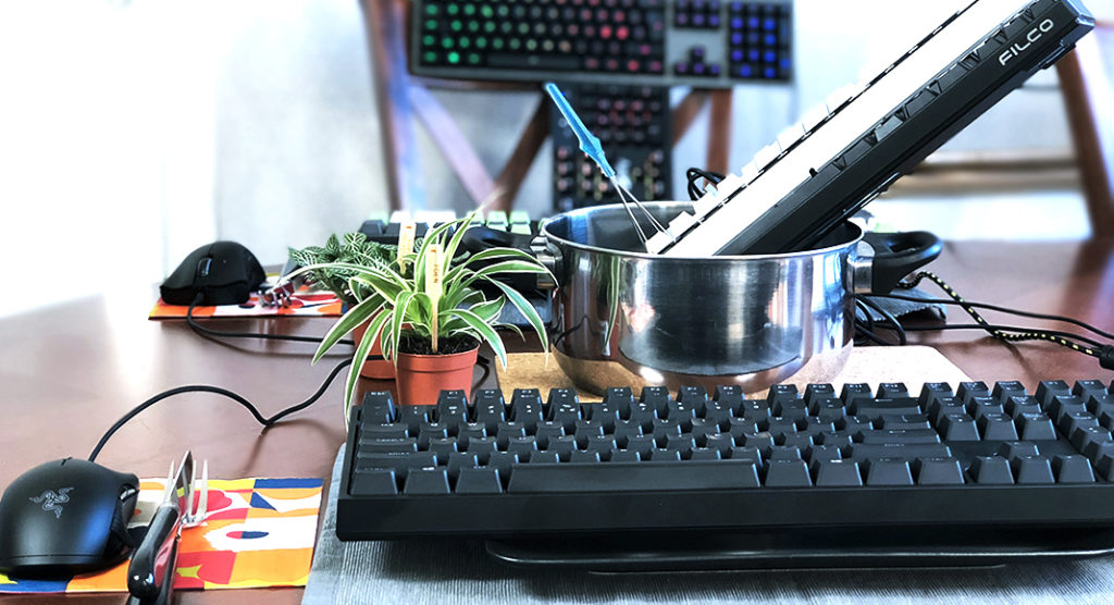
Svenska Tangentbordsguiden
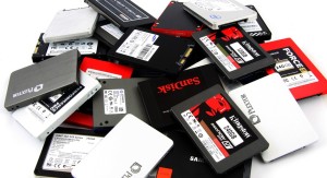
Svenska SSD-guiden
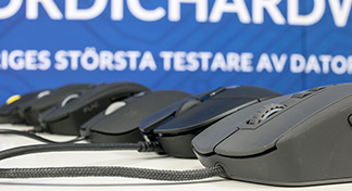
Svenska Musguiden

High End 2024: Audiovector Trapeze Ri – Audiovector ger finess & SLAM for the...
Audiovector Trapeze Ri är en ny högtalare som visas i samband med företagets 45-årsjubileum....

NordicHardware besöker High End Munich 2024!
Vi har väl besökt ett hundratal mässor och olika event under vår snart 25-åriga...

Asus ROG Ally X får större batteri och lagring
Innan det blir dags för en fullfjädrad uppföljare till ROG Ally kommer Asus sjösätta...

M4 iPad Pro är Apples tunnaste produkt hittills
Under sitt senaste event avtäckte Apple fyra nya iPad-surfplattor och den nya systemkretsen M4....